- 您現(xiàn)在的位置:買賣IC網(wǎng) > PDF目錄383941 > TDA8501T (NXP SEMICONDUCTORS) PAL/NTSC encoder PDF資料下載
參數(shù)資料
| 型號(hào): | TDA8501T |
| 廠商: | NXP SEMICONDUCTORS |
| 元件分類: | 顏色信號(hào)轉(zhuǎn)換 |
| 英文描述: | PAL/NTSC encoder |
| 中文描述: | COLOR SIGNAL ENCODER, PDSO24 |
| 封裝: | PLASTIC, SOT-137AH1, 24 PIN |
| 文件頁(yè)數(shù): | 9/30頁(yè) |
| 文件大小: | 238K |
| 代理商: | TDA8501T |
第1頁(yè)第2頁(yè)第3頁(yè)第4頁(yè)第5頁(yè)第6頁(yè)第7頁(yè)第8頁(yè)當(dāng)前第9頁(yè)第10頁(yè)第11頁(yè)第12頁(yè)第13頁(yè)第14頁(yè)第15頁(yè)第16頁(yè)第17頁(yè)第18頁(yè)第19頁(yè)第20頁(yè)第21頁(yè)第22頁(yè)第23頁(yè)第24頁(yè)第25頁(yè)第26頁(yè)第27頁(yè)第28頁(yè)第29頁(yè)第30頁(yè)
April 1993
9
Philips Semiconductors
Preliminary specification
PAL/NTSC encoder
TDA8501
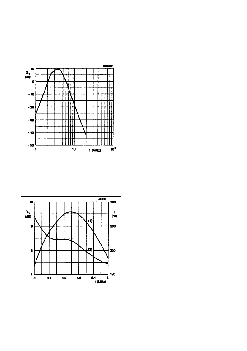
Fig.7
Band pass filter nominal frequency
response (NTSC mode).
Fig.8
Band pass filter nominal frequency/group
delay response (NTSC mode).
(1) frequency response.
(2) group delay.
Y +SYNC, CVBS
AND
C
HROMINANCE OUTPUTS
The Y signal from the matrix, or the Y signal from pin 5,
(selected via the switch) is added with the composite sync
signal of the sync separator (dependent on pin 17
conditioning). The output of the adder, nominal 1 V
(peak-to-peak), is connected to pin 22 (see Fig.1). Pin 22
is connected to an external delay line.
The delay line is necessary for correct timing of the
Y + SYNC signal with the chrominance signal. The output
resistor of the delay line is connected to V
REF
(pin 13). The
output of the external delay line is connected to (input)
pin 20.
The Y +SYNC (delayed) input signal at pin 20 is amplified
via a buffer to a level of 2 V (peak-to-peak) nominal and
connected to pin 19 (Y + SYNC output).
The Y
+
SYNC (delayed) input signal at pin 20 is also
connected via an internal resistor of 2 k
to the input of the
CVBS adder stage. After the internal resistor of 2 k
, and
before the input of the CVBS adder, an external notch filter
can be connected via pin 18.
The chrominance output of the bandpass filter is added
with Y +SYNC signal via the CVBS adder. The CVBS
(combined video and blanking signal) output of the adder
is connected to pin 16 with a nominal amplitude of 2 V
(peak-to-peak).
The chrominance output of the bandpass filter is amplified
via a buffer and connected to pin 14. The chrominance
amplitude corresponds with the value of Y + SYNC signal
output at pin 19. Together both outputs give the
Y +C (SVHS) signals.
B
LACK AND
B
LANKING LEVELS IN
PAL
AND
NTSC
MODES
PAL mode: Fig.9 illustrates the nominal Y + SYNC signal
at pin 22, the difference between black and blanking level
is 0 mV.
NTSC mode: Fig.10 illustrates the nominal Y + SYNC
signal at pin 22, the difference between black and blanking
level is 53 mV.
Because of the difference between the black and blanking
level in the NTSC mode, there are two options for NTSC.
相關(guān)PDF資料 |
PDF描述 |
|---|---|
| TDA8505 | SECAM encoder |
| TDA8510 | 26 W BTL and 2 x 13 W SE power amplifiers |
| TDA8510J | 26 W BTL and 2 x 13 W SE power amplifiers |
| TDA8511 | 4 x 13 W single-ended power amplifiers |
| TDA8511J | 4 x 13 W single-ended power amplifiers |
相關(guān)代理商/技術(shù)參數(shù) |
參數(shù)描述 |
|---|---|
| TDA8505 | 制造商:PHILIPS 制造商全稱:NXP Semiconductors 功能描述:SECAM encoder |
| TDA8510 | 制造商:PHILIPS 制造商全稱:NXP Semiconductors 功能描述:26 W BTL and 2 x 13 W SE power amplifiers |
| TDA8510J | 制造商:PHILIPS 制造商全稱:NXP Semiconductors 功能描述:26 W BTL and 2 x 13 W SE power amplifiers |
| TDA8510J/N2,112 | 功能描述:音頻放大器 AMP POWER 26W 17-SIL RoHS:否 制造商:STMicroelectronics 產(chǎn)品:General Purpose Audio Amplifiers 輸出類型:Digital 輸出功率: THD + 噪聲: 工作電源電壓:3.3 V 電源電流: 最大功率耗散: 最大工作溫度: 安裝風(fēng)格:SMD/SMT 封裝 / 箱體:TQFP-64 封裝:Reel |
| TDA8511 | 制造商:PHILIPS 制造商全稱:NXP Semiconductors 功能描述:4 x 13 W single-ended power amplifiers |
發(fā)布緊急采購(gòu),3分鐘左右您將得到回復(fù)。