- 您現(xiàn)在的位置:買賣IC網(wǎng) > PDF目錄383941 > TDA8350Q (NXP SEMICONDUCTORS) DC-coupled vertical deflection and East-West output circuit PDF資料下載
參數(shù)資料
| 型號: | TDA8350Q |
| 廠商: | NXP SEMICONDUCTORS |
| 元件分類: | 偏轉(zhuǎn) |
| 英文描述: | DC-coupled vertical deflection and East-West output circuit |
| 中文描述: | VERTICAL DEFLECTION IC, PZIP13 |
| 封裝: | POWER, PLASTIC, SOT-141-6, DIL-BENT-SIL, 13 PIN |
| 文件頁數(shù): | 4/16頁 |
| 文件大小: | 115K |
| 代理商: | TDA8350Q |
January 1995
4
Philips Semiconductors
Preliminary specification
DC-coupled vertical deflection and
East-West output circuit
TDA8350Q
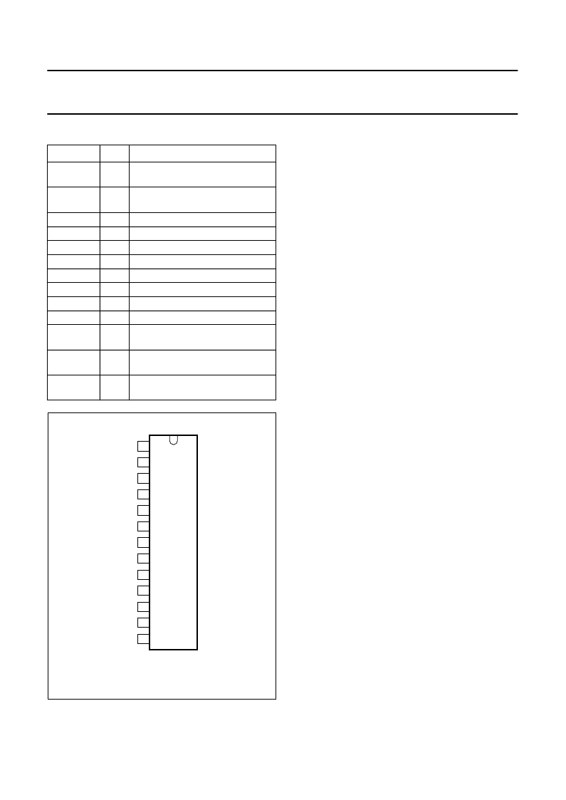
PINNING
SYMBOL
PIN
DESCRIPTION
I
drive(pos)
1
input power-stage (positive);
includes I
I(sb)
signal bias
input power-stage (negative);
includes I
I(sb)
signal bias
feedback voltage input
supply voltage
output voltage B
not connected
ground
flyback supply voltage
output voltage A
guard output voltage
East-West amplifier driver (sink)
output voltage
East-West amplifier input
correction current (negative)
East-West amplifier set input
current (positive)
I
drive(neg)
2
V
I(fb)
V
P
V
O(B)
n.c.
GND
V
FB
V
O(A)
V
O(guard)
V
O(sink)
3
4
5
6
7
8
9
10
11
I
I(corr)
12
I
I(set)
13
Fig.2 Pin configuration.
dbook, halfpage
TDA8350
Idrive(pos)
VI(fb)
VP
VO(B)
n.c.
GND
VFB
VO(A)
VO(guard)
VO(sink)
II(corr)
II(set)
Idrive(neg)
MBC226-1
1
2
3
4
5
6
7
8
9
10
11
12
13
FUNCTIONAL DESCRIPTION
The vertical driver circuit is a bridge configuration. The
deflection coil is connected between the output amplifiers,
which are driven in phase opposition. An external resistor
(R
M
) connected in series with the deflection coil provides
internal feed back information. The differential input circuit
is voltage driven. The input circuit has been adapted to
enable it to be used with the TDA9150, TDA9151B,
TDA9160A, TDA9162, TDA8366 and TDA8367 which
deliver symmetrical current signals. An external resistor
(R
CON
) connected between the differential input
determines the output current through the deflection coil.
The relationship between the differential input current and
the output current is defined by: I
diff
×
R
CON
= I
(coil)
×
R
M
.
The output current is adjustable from 0.5 A (p-p) to 3 A
(p-p) by varying R
M
. The maximum input differential
voltage is 1.8 V. In the application it is recommended that
V
diff
= 1.5 V (typ). This is recommended because of the
spread of input current and the spread in the value of
R
CON
.
The flyback voltage is determined by an additional supply
voltage V
FB
. The principle of operating with two supply
voltages (class G) makes it possible to fix the supply
voltage V
P
optimum for the scan voltage and the second
supply voltage V
FB
optimum for the flyback voltage. Using
this method, very high efficiency is achieved.
The supply voltage V
FB
is almost totally available as
flyback voltage across the coil, this being possible due to
the absence of a decoupling capacitor (not necessary, due
to the bridge configuration). The output circuit is fully
protected against the following:
thermal protection
short-circuit protection of the output pins (pins 5 and 9)
short-circuit of the output pins to V
P.
A guard circuit V
O(guard)
is provided. The guard circuit is
activated at the following conditions:
during flyback
during various short-circuit possibilities at the output
pins
during open loop
when the thermal protection is activated.
This signal can be used for blanking the picture tube
screen.
An East-West amplifier is also provided. This amplifier is
an inverting amplifier which is current driven with sink
current only capabilities.
相關(guān)PDF資料 |
PDF描述 |
|---|---|
| TDA8351 | DC-coupled vertical deflection circuit |
| TDA8376 | I2C-bus controlled PAL/NTSC TV processors |
| TDA8376A | I2C-bus controlled PAL/NTSC TV processors |
| TDA8376AH | I2C-bus controlled PAL/NTSC TV processors |
| TDA8380 | Control circuit for switched mode power supplies |
相關(guān)代理商/技術(shù)參數(shù) |
參數(shù)描述 |
|---|---|
| TDA8350Q/N6,112 | 功能描述:IC DC COUPLED V-DEFL 13-SIL RoHS:是 類別:集成電路 (IC) >> 專用 IC 系列:* 產(chǎn)品培訓(xùn)模塊:Lead (SnPb) Finish for COTS Obsolescence Mitigation Program 標(biāo)準(zhǔn)包裝:1 系列:- 類型:調(diào)幀器 應(yīng)用:數(shù)據(jù)傳輸 安裝類型:表面貼裝 封裝/外殼:400-BBGA 供應(yīng)商設(shè)備封裝:400-PBGA(27x27) 包裝:散裝 |
| TDA8351 | 制造商:PHILIPS 制造商全稱:NXP Semiconductors 功能描述:DC-coupled vertical deflection circuit |
| TDA8351/N6,112 | 功能描述:IC DC COUPLED V-DEFL 9-SIL RoHS:是 類別:集成電路 (IC) >> 專用 IC 系列:* 產(chǎn)品培訓(xùn)模塊:Lead (SnPb) Finish for COTS Obsolescence Mitigation Program 標(biāo)準(zhǔn)包裝:1 系列:- 類型:調(diào)幀器 應(yīng)用:數(shù)據(jù)傳輸 安裝類型:表面貼裝 封裝/外殼:400-BBGA 供應(yīng)商設(shè)備封裝:400-PBGA(27x27) 包裝:散裝 |
| TDA8351A | 制造商:PHILIPS 制造商全稱:NXP Semiconductors 功能描述:DC-coupled vertical deflection output circuit |
| TDA8351AQ | 制造商:PHILIPS 制造商全稱:NXP Semiconductors 功能描述:DC-coupled vertical deflection output circuit |
發(fā)布緊急采購,3分鐘左右您將得到回復(fù)。