- 您現(xiàn)在的位置:買賣IC網(wǎng) > PDF目錄383989 > TDA4884 (NXP SEMICONDUCTORS) Advanced monitor video controller for OSD PDF資料下載
參數(shù)資料
| 型號(hào): | TDA4884 |
| 廠商: | NXP SEMICONDUCTORS |
| 元件分類: | 音頻/視頻放大 |
| 英文描述: | Advanced monitor video controller for OSD |
| 中文描述: | 3 CHANNEL, VIDEO PREAMPLIFIER, PDIP20 |
| 封裝: | 0.300 INCH, PLASTIC, SOT-146-1, DIP-20 |
| 文件頁數(shù): | 5/28頁 |
| 文件大?。?/td> | 189K |
| 代理商: | TDA4884 |
第1頁第2頁第3頁第4頁當(dāng)前第5頁第6頁第7頁第8頁第9頁第10頁第11頁第12頁第13頁第14頁第15頁第16頁第17頁第18頁第19頁第20頁第21頁第22頁第23頁第24頁第25頁第26頁第27頁第28頁
1997 Nov 26
5
Philips Semiconductors
Product specification
Three gain control video pre-amplifier for OSD
TDA4884
6
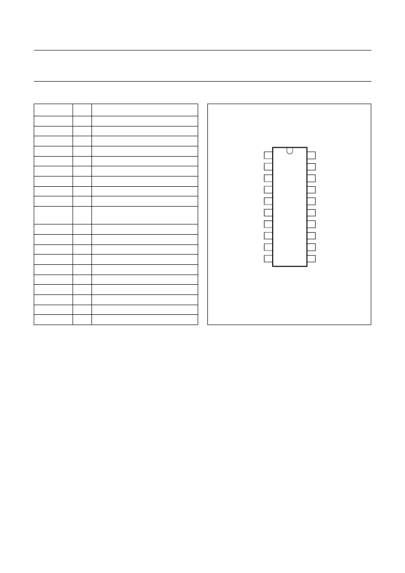
PINNING
SYMBOL
PIN
DESCRIPTION
GC2
VIN1
GC1
GND
VIN2
CC
V
P
VIN3
HBL
CL
1
2
3
4
5
6
7
8
9
gain control channel 2
signal input channel 1
gain control channel 1
ground
signal input channel 2
contrast control, OSD switch
supply voltage
signal input channel 3
horizontal blanking, switch-off
input clamping, vertical blanking,
test mode
gain control channel 3
feedback channel 3
voltage output channel 3
current output channel 3
feedback channel 2
voltage output channel 2
current output channel 2
feedback channel 1
voltage output channel 1
current output channel 1
10
GC3
FB3
VOUT3
IOUT3
FB2
VOUT2
IOUT2
FB1
VOUT1
IOUT1
11
12
13
14
15
16
17
18
19
20
Fig.2 Pin configuration.
handbook, halfpage
GC2
GND
CC
HBL
CL
VOUT1
IOUT1
FB1
VOUT2
IOUT2
FB2
VOUT3
VIN1
VIN2
VIN3
VP
IOUT3
FB3
GC3
GC1
1
2
3
4
5
6
7
8
9
10
11
12
20
19
18
17
16
15
14
13
TDA4884
MHA918
7
FUNCTIONAL DESCRIPTION
The RGB input signals 0.7 V (p-p) are capacitively coupled
into the TDA4884 (pins 2, 5 and 8) from a low ohmic
source and are clamped to an internal DC voltage (artificial
black level). Composite signals will not disturb normal
operations because an internal clipping circuit cuts all
signal parts below black level. All channels have a
maximum total voltage gain of 7 dB (maximum contrast
and maximum individual channel gain). With the nominal
channel gain of 1 dB and nominal contrast setting the
nominal black-to-white output amplitude is 0.79 V (p-p).
DC voltages are used for contrast and gain control.
7.1
Contrast control
Contrast control is achieved by a voltage at pin 6 and
affects the three channels simultaneously. To provide the
correct white point, an individual gain control (pins 3, 1 and
11) adjusts the signals of channels 1, 2 and 3.
7.2
Output stages
Each output stage provides a current output (pins 20, 17
and 14) and a voltage output (pins 19, 16 and 13). External
cascode transistors reduce power consumption of the IC
and prevent breakdown of the output transistors. Signal
output currents and peaking characteristics are
determined by external components at the voltage outputs
and the video supply. The channels have separate internal
feedback loops which ensure large signal linearity and
marginal signal distortion irrespective of output transistor
thermal V
BE
variation.
7.3
Input clamping
The clamping pulse (pin 10) is used for input clamping
only. The input signals have to be at black level during the
clamping pulse and are clamped to an internal artificial
black level. The coupling capacitors are used in this way
for black-level storage. Because the threshold for the
clamping pulse is higher than that for vertical blanking
(pin 10) the rise and fall times of the clamping pulse need
相關(guān)PDF資料 |
PDF描述 |
|---|---|
| TDA4885 | 150 MHz video controller with I2C-bus |
| TDA4886A | 140 MHz video controller with I2C-bus |
| TDA4886 | 140 MHz video controller with I2C-bus |
| TDA4887 | 160 MHz bus-controlled monitor video preamplifier |
| TDA4887PS | 160 MHz bus-controlled monitor video preamplifier |
相關(guān)代理商/技術(shù)參數(shù) |
參數(shù)描述 |
|---|---|
| TDA4885 | 制造商:未知廠家 制造商全稱:未知廠家 功能描述: |
| TDA4885/V2 | 制造商:NXP Semiconductors 功能描述: |
| TDA4886 | 制造商:PHILIPS-SEMI 功能描述: |
| TDA4886A | 制造商:PHILIPS 制造商全稱:NXP Semiconductors 功能描述:140 MHz video controller with I2C-bus |
| TDA4887 | 制造商:PHILIPS 制造商全稱:NXP Semiconductors 功能描述:160 MHz bus-controlled monitor video preamplifier |
發(fā)布緊急采購,3分鐘左右您將得到回復(fù)。