- 您現(xiàn)在的位置:買(mǎi)賣(mài)IC網(wǎng) > PDF目錄371180 > TDA10021 (NXP Semiconductors N.V.) DVB-C channel receiver PDF資料下載
參數(shù)資料
| 型號(hào): | TDA10021 |
| 廠商: | NXP Semiconductors N.V. |
| 英文描述: | DVB-C channel receiver |
| 中文描述: | DVB - C的通道接收機(jī) |
| 文件頁(yè)數(shù): | 8/16頁(yè) |
| 文件大小: | 92K |
| 代理商: | TDA10021 |
第1頁(yè)第2頁(yè)第3頁(yè)第4頁(yè)第5頁(yè)第6頁(yè)第7頁(yè)當(dāng)前第8頁(yè)第9頁(yè)第10頁(yè)第11頁(yè)第12頁(yè)第13頁(yè)第14頁(yè)第15頁(yè)第16頁(yè)
2001 Oct 01
8
Philips Semiconductors
Product specification
DVB-C channel receiver
TDA10021HT
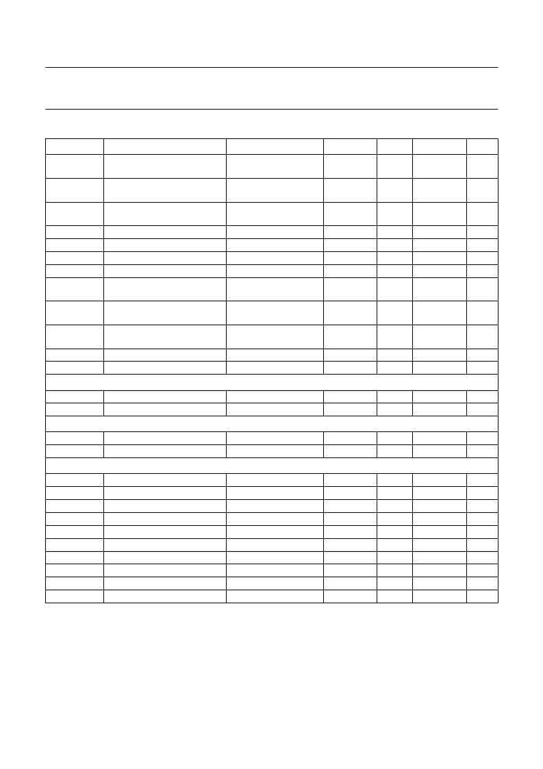
CHARACTERISTICS
Notes
1.
The voltage level of the 5 V supply must always exceed or at least equal the voltage level of the 3.3 V supply during
power-up and power-down in order to guarantee protection against latch-up.
All digital inputs are 5 V tolerant except pin XIN.
I
OH
, I
OL
=
±
4 mA for pins SACLK, SCL, SDA, SDAT, SCLT, TCK, TDI, TRST, TMS, TDO, GPIO, UNCOR, PSYNC,
OCLK, DEN and DO[7:0]. For all other pins, I
OH
, I
OL
=
±
2 mA.
2.
3.
SYMBOL
V
DDD33
PARAMETER
CONDITIONS
V
DDD
= 3.3 V
±
10%
MIN.
TYP.
3.3
MAX.
UNIT
V
digital supply voltage for the
pads
digital supply voltage for the
core
digital supply voltage
2.97
3.63
V
DDD18
V
DDD
= 1.8 V
±
5%
1.7
1.8
1.9
V
V
DDD50
only for 5 V
requirements; note 1
TTL input; note 2
TTL input
note 3
4.75
5.0
5.25
V
V
IH
V
IL
V
OH
V
OL
I
DDD33
HIGH-level input voltage
LOW-level input voltage
HIGH-level output voltage
LOW-level output voltage
digital supply current for the
pads
digital supply current for the
core
total power dissipation
2
0
2.4
46
V
DDD50
0.8
0.4
V
V
V
V
mA
f
s
= 28.92 MHz;
symbol rate = 7 Mbaud
f
s
= 28.92 MHz;
symbol rate = 7 Mbaud
f
s
= 28.92 MHz;
symbol rate = 7 Mbaud
I
DDD18
120
mA
P
tot
540
mW
C
i
T
amb
XTAL; pin XIN
V
IH
V
IL
PLL
V
DDD(PLL)
V
DDA(PLL)
ADC
V
DDA1
V
DDA2
,V
DDA3
V
IP
,V
IM
V
i
V
ref(pos)
V
ref(neg)
V
offset
R
i
C
i
B
input capacitance
ambient temperature
0
5
70
pF
°
C
HIGH-level input voltage
LOW-level input voltage
0.7V
DDD33
0
V
DDD33
0.3V
DDD33
V
V
digital PLL supply voltage
analog PLL supply voltage
V
DDD
= 1.8 V
±
5%
V
DDA
= 3.3 V
±
10%
1.7
2.97
1.8
3.3
1.9
3.63
V
V
analog ADC supply voltage
analog ADC supply voltage
analog ADC inputs
signal input range
positive reference voltage
negative reference voltage
input offset voltage
input resistance (V
IP
or V
IM
)
input capacitance (V
IP
or V
IM
)
input full power bandwidth
V
DDA
= 1.8 V
±
5%
V
DDA
= 3.3 V
±
10%
1.7
2.97
0.5
0.5 to
1.0
1.95
0.95
25
40
1.8
3.3
2.15
1.15
10
5
50
1.9
3.63
V
DDA3
+ 0.5
+0.5 to +1.0
2.35
1.35
+25
10
V
V
V
V
V
V
mV
k
pF
MHz
I
R
= V
IP
V
IM
3 dB bandwidth
相關(guān)PDF資料 |
PDF描述 |
|---|---|
| TDA10021HT | DVB-C channel receiver |
| TDA10045 | DVB-T channel receiver |
| TDA10045H | DVB-T channel receiver |
| TDA1005A | FREQUENCY MULTIPLEX PLL STEREO DECODER |
| TDA1005AT | FREQUENCY MULTIPLEX PLL STEREO DECODER |
相關(guān)代理商/技術(shù)參數(shù) |
參數(shù)描述 |
|---|---|
| TDA10021HT | 制造商:PHILIPS 制造商全稱:NXP Semiconductors 功能描述:DVB-C channel receiver |
| TDA10023HT/C1,518 | 制造商:Entropic Communications 功能描述:935273244518-R43 |
| TDA10025 | 制造商:NXP 功能描述:Dual cable demodulator |
| TDA10025HN/C1,518 | 功能描述:調(diào)節(jié)器/解調(diào)器 Dual Cable (QAM) Demodulator RoHS:否 制造商:Texas Instruments 封裝 / 箱體:PVQFN-N24 封裝:Reel |
| TDA10025HN/C1,551 | 功能描述:調(diào)節(jié)器/解調(diào)器 DUAL CBL DEMODULATOR RoHS:否 制造商:Texas Instruments 封裝 / 箱體:PVQFN-N24 封裝:Reel |
發(fā)布緊急采購(gòu),3分鐘左右您將得到回復(fù)。