- 您現(xiàn)在的位置:買賣IC網(wǎng) > PDF目錄383938 > TCM812SERC (Microchip Technology Inc.) 4-Pin Microcontroller Reset Monitors PDF資料下載
參數(shù)資料
| 型號: | TCM812SERC |
| 廠商: | Microchip Technology Inc. |
| 英文描述: | 4-Pin Microcontroller Reset Monitors |
| 中文描述: | 4引腳單片機復位監(jiān)控器 |
| 文件頁數(shù): | 4/14頁 |
| 文件大小: | 258K |
| 代理商: | TCM812SERC |
TCM811/TCM812
DS21615B-page 4
2002 Microchip Technology Inc.
2.0
APPLICATIONS INFORMATION
The TCM811/TCM812 provides accurate V
DD
monitor-
ing and reset timing during power-up, power-down, and
brownout/sag conditions. These devices also reject
negative-going transients (glitches) on the power sup-
ply line. Figure 2-1 shows the maximum transient dura-
tion vs. maximum negative excursion (overdrive) for
glitch rejection. Any combination of duration and over-
drive that is under the curve will not generate a reset
signal. Combinations above the curve are detected as
a brownout or power-down. Transient immunity can be
improved by adding a 0.1 μF capacitor in close proxim-
ity to the V
DD
pin of the TCM811/812.
FIGURE 2-1:
Overdrive for Glitch Rejection at 25°C.
Maximum
Transient
Duration vs.
2.1
RESET Signal Integrity During Power-
Down
The TCM811 RESET push-pull output is valid to V
DD
=
1.0V. Below this voltage the output becomes an "open
circuit" and does not sink current. This means CMOS
logic inputs to the microcontroller will be floating at an
undetermined voltage. Most digital systems are com-
pletely shutdown well above this voltage. However, in
situations where RESET must be maintained valid to
V
DD
= 0V, a pull-down resistor must be connected from
RESET to ground to discharge stray capacitances and
hold the output low (Figure 2-2). This resistor value,
though not critical, should be chosen such that it does
not appreciably load RESET under normal operation
(100 k
will be suitable for most applications). Simi-
larly, a pull-up resistor to V
DD
is required for the
TCM812 to ensure a valid high RESET for V
DD
below
1.1V.
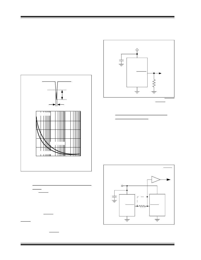
FIGURE 2-2:
output of the TCM811 ensures that the RESET output
is valid to V
DD
= 0V.
The addition of R
1
at the RESET
2.2
Controllers and Processors With
Bidirectional I/O Pins
Some microcontrollers have bi-directional reset pins.
Depending on the current drive capability of the control-
ler pin, an indeterminate logic level may result if there
is a logic conflict. This can be avoided by adding a
4.7 k
resistor in series with the output of the TCM811/
TCM812 (Figure 2-3). If there are other components in
the system which require a reset signal, they should be
buffered so as not to load the reset line. If the other
components are required to follow the reset I/O of the
microcontroller, the buffer should be connected as
shown with the solid line.
FIGURE 2-3:
directional Reset I/O.
Interfacing the TCM811 to a Bi-
RESET COMPARATOR OVERDRIVE,
VTH - VDD (mV)
400
240
160
320
80
0
1
10
100
1000
M
T
A
= +25C
V
TH
Duration
Overdrive =
V
D D
V
DD
TCM81xL/M
TCM81xR/S/T
TCM811
RESET
V
DD
V
DD
R
1
100 k
GND
4
2
0.1μF
1
TCM811
V
DD
RESET
GND
RESET
GND
Buffered RESET
To Other System
Components
BUFFER
Micro
controller
4.7 k
0.1μF
4
2
1
相關PDF資料 |
PDF描述 |
|---|---|
| TCM811LERC | 4-Pin Microcontroller Reset Monitors |
| TCM812LERC | 4-Pin Microcontroller Reset Monitors |
| TCM811TERC | 4-Pin Microcontroller Reset Monitors |
| TCM812RERC | 4-Pin Microcontroller Reset Monitors |
| TCM812TERC | 4-Pin Microcontroller Reset Monitors |
相關代理商/技術參數(shù) |
參數(shù)描述 |
|---|---|
| TCM812SERCTR | 功能描述:監(jiān)控電路 4-Pin uP 2.93V Reset RoHS:否 制造商:STMicroelectronics 監(jiān)測電壓數(shù): 監(jiān)測電壓: 欠電壓閾值: 過電壓閾值: 輸出類型:Active Low, Open Drain 人工復位:Resettable 監(jiān)視器:No Watchdog 電池備用開關:No Backup 上電復位延遲(典型值):10 s 電源電壓-最大:5.5 V 最大工作溫度:+ 85 C 安裝風格:SMD/SMT 封裝 / 箱體:UDFN-6 封裝:Reel |
| TCM812TERC | 制造商:MICROCHIP 制造商全稱:Microchip Technology 功能描述:4-Pin Microcontroller Reset Monitors |
| TCM812TERCTR | 功能描述:監(jiān)控電路 4-Pin uP 38V Reset RoHS:否 制造商:STMicroelectronics 監(jiān)測電壓數(shù): 監(jiān)測電壓: 欠電壓閾值: 過電壓閾值: 輸出類型:Active Low, Open Drain 人工復位:Resettable 監(jiān)視器:No Watchdog 電池備用開關:No Backup 上電復位延遲(典型值):10 s 電源電壓-最大:5.5 V 最大工作溫度:+ 85 C 安裝風格:SMD/SMT 封裝 / 箱體:UDFN-6 封裝:Reel |
| TCM8230MD | 制造商:TOSHIBA 制造商全稱:Toshiba Semiconductor 功能描述:VGA CAMERA MODULE |
| TCM8230MDA | 制造商:TOSHIBA 制造商全稱:Toshiba Semiconductor 功能描述:VGA CAMERA MODULE |
發(fā)布緊急采購,3分鐘左右您將得到回復。