- 您現(xiàn)在的位置:買賣IC網(wǎng) > PDF目錄361412 > TC835CBU (TelCom Semiconductor, Inc.) PERSONAL COMPUTER DATA ACQUISITION A/D CONVERTER PDF資料下載
參數(shù)資料
| 型號(hào): | TC835CBU |
| 廠商: | TelCom Semiconductor, Inc. |
| 英文描述: | PERSONAL COMPUTER DATA ACQUISITION A/D CONVERTER |
| 中文描述: | 個(gè)人計(jì)算機(jī)數(shù)據(jù)采集的A / D轉(zhuǎn)換器 |
| 文件頁數(shù): | 8/12頁 |
| 文件大小: | 206K |
| 代理商: | TC835CBU |
3-72
TELCOM SEMICONDUCTOR, INC.
PERSONAL COMPUTER
DATA ACQUISITION A/D CONVERTER
TC835
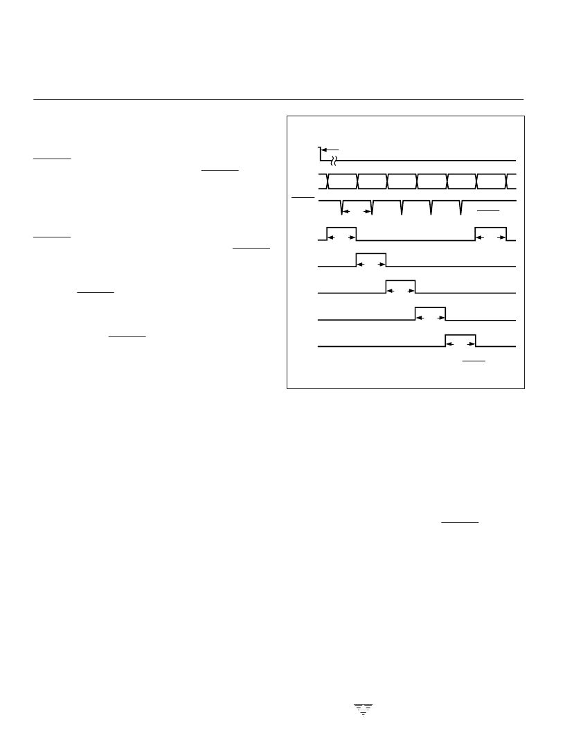
The new measurement cycle begins with a 10,001-
count auto-zero phase. At the end of this phase the busy
signal goes high.
STROBE Output
(Pin 26)
During the measurement cycle, the STROBE control
line is pulsed low five times. The five low pulses occur in the
center of the digit drive signals (D
1
, D
2
, D
3
, D
5
, Figure 8).
D
5
(MSD) goes high for 201 counts when the measure-
ment cycles end. In the center of the D
5
pulse, 101 clock
pulses after the end of the measurement cycle, the first
STROBE occurs for one-half clock pulse. After the D
5
digit
strobe, D
4
goes high for 200 clock pulses. The STROBE
goes low 100 clock pulses after D
4
goes high. This continues
through the D
1
digit drive pulse.
The digit drive signals will continue to permit display
scanning. STROBE pulses are not repeated until a new
measurement is completed. The digit drive signals will not
continue if the previous signal resulted in an overrange
condition.
The active low STROBE pulses aid BCD data transfer to
UARTs, processors and external latches. (See Application
Note 16.)
BUSY Output
(Pin 21)
At the beginning of the signal-integration phase, BUSY
goes high and remains high until the first clock pulse after the
integrator zero crossing. BUSY returns to the logic "0" state
after the measurement cycle ends in an overrange condi-
tion. The internal display latches are loaded during the first
clock pulse after BUSY, and are latched at the clock pulse
end. The BUSY signal does not go high at the beginning of
the measurement cycle, which starts with the auto-zero
cycle.
OVERRANGE Output
(Pin 27)
If the input signal causes the reference voltage integra-
tion time to exceed 20,000 clock pulses, the OVERRANGE
output is set to a logic "1." The overrange output register is
set when BUSY goes low, and is reset at the beginning of the
next reference-integration phase.
UNDERRANGE Output
(Pin 28)
If the output count is 9% of full scale or less (
≤
1800
counts), the underrange register bit is set at the end of
BUSY. The bit is set low at the next signal-integration phase.
POLARITY Output
(Pin 23)
A positive input is registered by a logic "1" polarity signal.
The polarity bit is valid at the beginning of reference inte-
grate and remains valid until determined during the next
conversion.
Figure 8. Strobe Signal Pulses Low Five Times per Conversion
END OF CONVERSION
D5 (MSD)
DATA
BUSY
B1–B8
STROBE
D5
D4
D3
D2
D1
D4
DATA
D3
DATA
D2
DATA
D1 (LSD)
DATA
D5
DATA
NOTE ABSENCE
OF STROBE
201
COUNTS
200
COUNTS
200
COUNTS
200
COUNTS
200
COUNTS
200
COUNTS
200
COUNTS
*
*
DELAY BETWEEN BUSY GOING LOW AND FIRST STROBE
PULSE IS DEPENDENT ON ANALOG INPUT.
TC835
OUTPUTS
The polarity bit is valid even for a zero reading. Signals
less than the converter's LSB will have the signal polarity
determined correctly. This is useful in null applications.
DIGIT Drive Outputs
(Pins 12, 17, 18, 19 and 20)
Digit drive signals are positive-going signals. The scan
sequence is D
5
to D
1
. All positive pulses are 200 clock pulses
wide, except D
5
, which is 201 clock pulses wide.
All five digits are scanned continuously, unless an
overrange condition occurs. In an overrange condition, all
digit drives are held low from the final STROBE pulse until
the beginning of the next reference-integrate phase. The
scanning sequence is then repeated. This provides a blink-
ing visual display indication.
BCD Data Outputs
(Pins 13, 14, 15 and 16)
The binary coded decimal (BCD) bits B
8
, B
4
, B
2
, B
1
, are
positive-true logic signals. The data bits become active
simultaneously with the digit drive signals. In an overrange
condition, all data bits are at a logic "0" state.
相關(guān)PDF資料 |
PDF描述 |
|---|---|
| TC835CBU | Personal Computer Data Acquisition A/D Converter |
| TC835CPI | Personal Computer Data Acquisition A/D Converter |
| TC835 | Personal Computer Data Acquisition A/D Converter |
| TC835CKW | Personal Computer Data Acquisition A/D Converter |
| TC835CKW | PERSONAL COMPUTER DATA ACQUISITION A/D CONVERTER |
相關(guān)代理商/技術(shù)參數(shù) |
參數(shù)描述 |
|---|---|
| TC835CBU713 | 功能描述:LED顯示驅(qū)動(dòng)器 4.5 D BCD A/D-PC Dat RoHS:否 制造商:Micrel 數(shù)位數(shù)量:5 片段數(shù)量: 安裝風(fēng)格:SMD/SMT 封裝 / 箱體:PLCC-44 工作電源電壓:4.75 V to 11 V 最大電源電流:10 mA 最大工作溫度:+ 85 C 最小工作溫度:- 40 C 封裝:Tube |
| TC835CKW | 功能描述:LED顯示驅(qū)動(dòng)器 4.5 D BCD A/D-PC Dat RoHS:否 制造商:Micrel 數(shù)位數(shù)量:5 片段數(shù)量: 安裝風(fēng)格:SMD/SMT 封裝 / 箱體:PLCC-44 工作電源電壓:4.75 V to 11 V 最大電源電流:10 mA 最大工作溫度:+ 85 C 最小工作溫度:- 40 C 封裝:Tube |
| TC835CKW713 | 功能描述:LED顯示驅(qū)動(dòng)器 4.5 D BCD A/D-PC Dat RoHS:否 制造商:Micrel 數(shù)位數(shù)量:5 片段數(shù)量: 安裝風(fēng)格:SMD/SMT 封裝 / 箱體:PLCC-44 工作電源電壓:4.75 V to 11 V 最大電源電流:10 mA 最大工作溫度:+ 85 C 最小工作溫度:- 40 C 封裝:Tube |
| TC835CPI | 功能描述:LED顯示驅(qū)動(dòng)器 4.5 D BCD A/D-PC Dat RoHS:否 制造商:Micrel 數(shù)位數(shù)量:5 片段數(shù)量: 安裝風(fēng)格:SMD/SMT 封裝 / 箱體:PLCC-44 工作電源電壓:4.75 V to 11 V 最大電源電流:10 mA 最大工作溫度:+ 85 C 最小工作溫度:- 40 C 封裝:Tube |
| TC8395-90 | 制造商:未知廠家 制造商全稱:未知廠家 功能描述:16-Bit Microcontroller |
發(fā)布緊急采購,3分鐘左右您將得到回復(fù)。