- 您現(xiàn)在的位置:買賣IC網(wǎng) > PDF目錄361412 > TC826 (TelCom Semiconductor, Inc.) A/D CONVERTER WITH BAR GRAPH DISPLAY OUTPUT PDF資料下載
參數(shù)資料
| 型號(hào): | TC826 |
| 廠商: | TelCom Semiconductor, Inc. |
| 英文描述: | A/D CONVERTER WITH BAR GRAPH DISPLAY OUTPUT |
| 中文描述: | 的A / D轉(zhuǎn)換器條形圖顯示輸出 |
| 文件頁數(shù): | 9/12頁 |
| 文件大小: | 122K |
| 代理商: | TC826 |
3-179
TELCOM SEMICONDUCTOR, INC.
7
6
5
4
3
1
2
8
Auto-Zero Capacitor
(CAZ)
C
AZ
should be 2–3 times larger than the integration
capacitor. A polypropylene capacitor is suggested. Typical
values from 0.14
μ
F to 0.068
μ
F are satisfactory.
Reference Capacitor
(CREF)
A 1
μ
F capacitor is suggested. Low leakage capacitors
such as polypropylene are recommended.
Several capacitor/resistor combinations for common
full-scale input conditions are given in Table 1.
Table 1Suggested Component Values
2V
Full-Scale
Component V
REF
≈
1V
R
INT
2 M
C
INT
0.033
μ
F
C
REF
1
μ
F
C
AZ
0.068
μ
F
R
OSC
430k
200 mV
Full-Scale
V
REF
≈
100 mV V
REF
≈
10 mV
200k
0.033
μ
F
1
μ
F
0.068
μ
F
430k
20 mV
Full-Scale
20k
0.033
μ
F
1 F
0.14
μ
F
430k
NOTES:
Approximately 5 conversions/second.
Differential Signal Inputs
The TC826 is designed with true differential inputs and
accepts input signals within the input stage common–mode
voltage range (VCM). The typical range is V
+
–1 to V
–
+1V.
Common–mode voltages are removed from the system
when the TC826 operates from a battery or floating power
source (Isolated from measured system) and –IN is con-
nected to analog–common (V
COM
).
In systems where common–mode rejection ratio mini-
mizes error. Common–mode voltages do, however, affect
the integrator output level. Integrator output saturation must
be prevented. A worse case condition exists if a large
positive V
CM
exists in conjunction with a full–scale negative
differential signal. The negative signal drives the integrator
output positive along with V
CM
. For such applications, the
integrator output swing can be reduced below the recom-
mended 2V full–scale swing. The integrator output will swing
within 0.3V of V
DD
or V
SS
without increased linearity error.
Digital Section
The TC826 contains all the segment drivers necessary
to drive a liquid crystal display (LCD). An LCD backplane
driver is included. The backplane frequency is the external
clock frequency divided by 256. A 430k
OSC
gets the
backplane frequency to approximately 55Hz with a 5V
nominal amplitude. When a segment driver is in phase with
the backplane signal the segment is ‘OFF’. An out–of–phase
segment drive signal causes the segment to be ‘ON’ or
visible. This AC drive configuration results in negligible DC
The internal voltage reference potential availabe at
analog-common will normally be used to supply the convert-
ers reference. This potential is stable whenever the supply
potential is greater than approximately 7V. In applications
where an externally generated reference voltage is desired
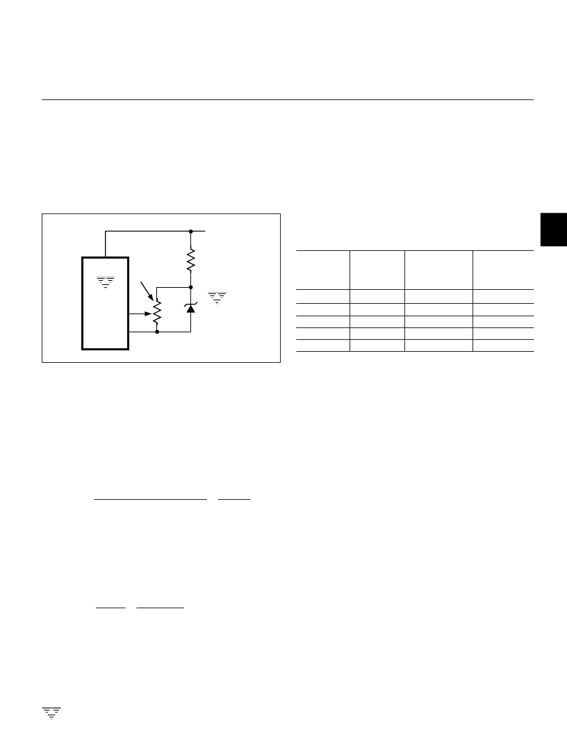
refer to Figure 6.
The reference voltage is adjusted with a near full-scale
input signal. Adjust for proper LCD display readout.
TC826
REF IN
ANALOG
COMMON
1.2V
REFERENCE
5
2
V+
8
TC9491CZM
V+
(b)
Figure 6. External Reference
Components Value Selection
Integrating Resistor
(RINT)
The desired full-scale input voltage and output current
capability of the input buffer and integrator amplifier set the
integration resistor value. The internal class A output stage
amplifiers will supply a 1
μ
A drive durrent with minimal
linearity error. R
INT
is easily calculated for a 1
μ
A full-scale
current:
R
INT
= Full-Scale Input Voltage (V) = VFS
1 x 10
–6
Where VFS = Full-Scale Analog Input
Integrating Capacitor
(CINT)
The integrating capacitor should be slected to maximize
intgrator output swing. The integrator output will swing to
within 0.4V of V
S+
or V
S–
without saturating.
The integrating capacitor is easily calculated:
C
INT
= VFS
640
Where :
V
INT
= Integrator Swing
F
OSC
= Oscillator Frequency
The integrating capacitor should be selected for low
dielectric absorption to prevent roll-over errors. Polypro-
pylene capacitors are suggested.
1 x10
–6
R
INT
(
F
OSC
x V
INT
)
TC826
A/D CONVERTER WITH
BAR GRAPH DISPLAY OUTPUT
相關(guān)PDF資料 |
PDF描述 |
|---|---|
| TC826CBU | Analog-to-Digital Converter with Bar Graph Display Output |
| TC826CBU | A/D CONVERTER WITH BAR GRAPH DISPLAY OUTPUT |
| TC835CBU | PERSONAL COMPUTER DATA ACQUISITION A/D CONVERTER |
| TC835CBU | Personal Computer Data Acquisition A/D Converter |
| TC835CPI | Personal Computer Data Acquisition A/D Converter |
相關(guān)代理商/技術(shù)參數(shù) |
參數(shù)描述 |
|---|---|
| TC826-0 | 制造商:Thomas & Betts 功能描述:CABLE TIES |
| TC826CBU | 制造商:Microchip Technology Inc 功能描述:ADC WITH BAR GRAPH DISPLAY OUTPUT |
| TC826-TB | 制造商:Thomas & Betts 功能描述:CABLE TIE MOUNT, NYLON 6.6, NATURAL; Mount Fixing Type:Screw; Mount Material:Nylon 6.6; Mount Color:Natural; Accessory Type:Mounting Base; For Use With:Cable Ties ;RoHS Compliant: Yes 制造商:Thomas & Betts 功能描述:Cable Accessories Two Direction Mounting Base Bulk |
| TC-827-SC | 制造商:Thomas & Betts 功能描述: |
| TC828-0 | 制造商:Thomas & Betts 功能描述:CABLE TIE MT .4X.9 2-DIR 8SCREW BLK |
發(fā)布緊急采購,3分鐘左右您將得到回復(fù)。