- 您現(xiàn)在的位置:買賣IC網(wǎng) > PDF目錄383935 > TC818 (Microchip Technology Inc.) Auto-Ranging Analog-to-Digital Converter with 3-1/2 Digit Display PDF資料下載
參數(shù)資料
| 型號(hào): | TC818 |
| 廠商: | Microchip Technology Inc. |
| 英文描述: | Auto-Ranging Analog-to-Digital Converter with 3-1/2 Digit Display |
| 中文描述: | 自動(dòng)測(cè)距模擬到數(shù)字轉(zhuǎn)換器與數(shù)字顯示3-1/2 |
| 文件頁(yè)數(shù): | 19/24頁(yè) |
| 文件大小: | 583K |
| 代理商: | TC818 |
第1頁(yè)第2頁(yè)第3頁(yè)第4頁(yè)第5頁(yè)第6頁(yè)第7頁(yè)第8頁(yè)第9頁(yè)第10頁(yè)第11頁(yè)第12頁(yè)第13頁(yè)第14頁(yè)第15頁(yè)第16頁(yè)第17頁(yè)第18頁(yè)當(dāng)前第19頁(yè)第20頁(yè)第21頁(yè)第22頁(yè)第23頁(yè)第24頁(yè)
2002 Microchip Technology Inc.
DS21475B-page 19
TC818A
Vendors for piezo electric audio transducers are:
Gulton Industries
Piezo Products Division
212 Durham Avenue
Metuchen, New Jersey 08840
(201) 548-2800
Typical P/Ns: 102-95NS, 101-FB-00
Taiyo Yuden (USA) Inc.
Arlington Center
714 West Algonquin Road
Arlington Heights, Illinois 60005
Typical P/Ns: CB27BB, CB20BB, CB355BB
3.18
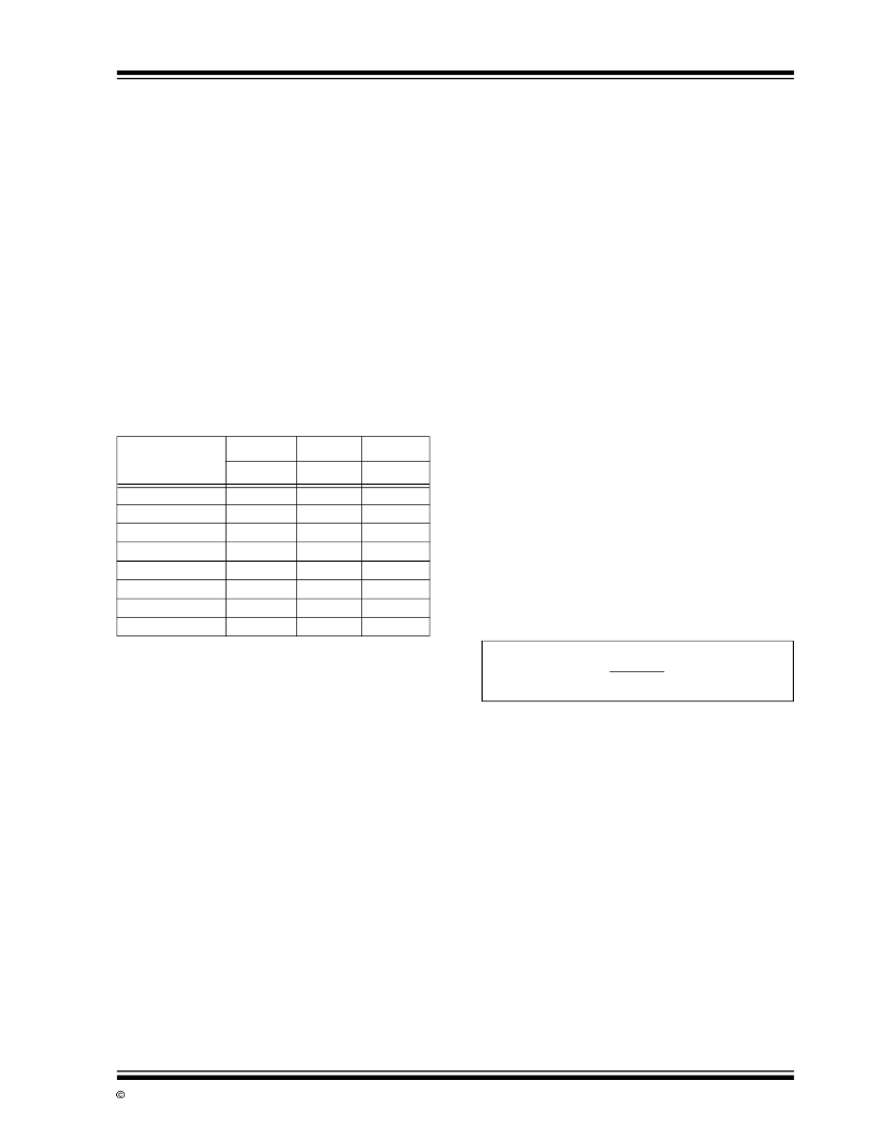
Display Decimal Point Selection
The TC818A provides a decimal point LCD drive sig-
nal. The decimal point position is a function of the
selected full scale range, as shown in Table 3-5.
3.19
AC-to-DC Converter Operational
Amplifier
The TC818A contains an on-chip operational amplifier
that may be connected as a rectifier for AC-to-DC volt-
age and current measurements. Typical operational
amplifier characteristics are:
Slew Rate: 1V/
μ
sec
Unity Gain Bandwidth: 0.4MHz
Open Loop Gain: 44dB
Output Voltage Swing (Load = 10k
) ± 1.5V
(Referenced to Analog Common)
When the AC measurement option is selected, the
input buffer receives an input signal through switch
S14, rather than switch S11 (see Figure 3-1). With
external circuits, the AC Operating mode can be used
to perform other types of functions within the con-
straints of the internal operational amplifier. External
circuits that perform true RMS conversion, or a peak
hold function, are typical examples.
3.20
Component Selection
3.20.1
INTEGRATION RESISTOR
SELECTION
The TC818A automatically selects one of two external
integration resistors. RVIBUF (Pin 55) is selected for
voltage and current measurement. R
BUF (Pin 54) is
selected for resistance measurements.
3.20.2
RVIBUF SELECTION (PIN 55)
In auto-range operation, the TC818A operates with a
200mV maximum full scale potential at V
I
(Pin 44).
Resistive dividers at VR2 (Pin 41), VR3 (Pin 40), VR4
(Pin 43), and VR5 (Pin 42) are automatically switched
to maintain the 200V full scale potential.
In Manual mode, the Extended Operating mode is acti-
vated, giving a 300mV full scale potential at V
I
(Pin 44).
The integrator output swing should be maximized, but
saturations must be avoided. The integrator will swing
within 0.45V of V
CC
(Pin 28) and 0.5V of V
SS
(Pin 57)
without saturating. A ±2V swing is suggested. The
value of RVIBUF is easily calculated, assuming a worst
case extended resolution input signal:
Where:
V
INT
= Integrator swing = ±2V
t
I
= Integration time = 100msec
C
I
= Integration capacitor = 0.1
μ
F
V
MAX
= Maximum input at V
I
= 300mV
EQUATION 3-1:
3.20.3
R
BUF SELECTION (PIN 54)
In ratiometric resistance measurements, the signal at
R
X
(Pin 50) is always positive, with respect to analog
common. The integrator swings negative.
The worst case integrator swing is for the 200
range
with the manual, extended resolution option.
The input voltage, V
X
(Pin 50) is easily calculated (see
Figure 3-15).
TABLE 3-5:
DECIMAL POINT SELECTION
Full Scale Range
1 * 9
* 9
* 9
DP3
DP2
DP1
2000V, 2000k
200V, 200k
20V, 20k
2V, 2k
200V, 200
200mV, 200
20mA
200mA
OFF
OFF
OFF
ON
OFF
OFF
OFF
OFF
OFF
OFF
ON
OFF
OFF
OFF
ON
OFF
OFF
ON
OFF
OFF
ON
ON
OFF
ON
RVIBUF =
V
MAX
(T
I
)
V
INT
(C
I
)
= 150k
相關(guān)PDF資料 |
PDF描述 |
|---|---|
| TC818ACBU | Auto-Ranging Analog-to-Digital Converter with 3-1/2 Digit Display |
| TCA7660 | HIGH FREQUENCY 7660 DC-TO-DC VOLTAGE CONVERTER |
| TCA785 | Phase Control IC |
| TCA785 | Phase Control IC |
| TCA830 | MONOLITHISH INTEGRIERTE SCHALTUNG MONOLITHIC INTEGRATED CIRCUIT |
相關(guān)代理商/技術(shù)參數(shù) |
參數(shù)描述 |
|---|---|
| TC818A | 制造商:MICROCHIP 制造商全稱:Microchip Technology 功能描述:Auto-Ranging Analog-to-Digital Converter with 3-1/2 Digit Display |
| TC818ACBU | 制造商:MICROCHIP 制造商全稱:Microchip Technology 功能描述:Auto-Ranging Analog-to-Digital Converter with 3-1/2 Digit Display |
| TC-819-SC | 制造商:Thomas & Betts 功能描述: |
| TC820 | 制造商:TELCOM 制造商全稱:TelCom Semiconductor, Inc 功能描述:3-3/4 DIGIT A/D CONVERTER WITH FREQUENCY COUNTER AND LOGIC PROBE |
| TC820CKW | 功能描述:LCD 驅(qū)動(dòng)器 3-3/4 A/D Converter RoHS:否 制造商:Maxim Integrated 數(shù)位數(shù)量:4.5 片段數(shù)量:30 最大時(shí)鐘頻率:19 KHz 工作電源電壓:3 V to 3.6 V 最大工作溫度:+ 85 C 最小工作溫度:- 20 C 封裝 / 箱體:PDIP-40 封裝:Tube |
發(fā)布緊急采購(gòu),3分鐘左右您將得到回復(fù)。