- 您現(xiàn)在的位置:買賣IC網 > PDF目錄98179 > TC7135C/LI 1-CH 4-BIT DUAL-SLOPE ADC, PARALLEL ACCESS, PQCC28 PDF資料下載
參數(shù)資料
| 型號: | TC7135C/LI |
| 元件分類: | ADC |
| 英文描述: | 1-CH 4-BIT DUAL-SLOPE ADC, PARALLEL ACCESS, PQCC28 |
| 封裝: | PLASTIC, LCC-28 |
| 文件頁數(shù): | 24/28頁 |
| 文件大?。?/td> | 443K |
| 代理商: | TC7135C/LI |
第1頁第2頁第3頁第4頁第5頁第6頁第7頁第8頁第9頁第10頁第11頁第12頁第13頁第14頁第15頁第16頁第17頁第18頁第19頁第20頁第21頁第22頁第23頁當前第24頁第25頁第26頁第27頁第28頁
2007 Microchip Technology Inc.
DS21460D-page 5
TC7135
2.0
PIN DESCRIPTIONS
The description of the pins are listed in Table 2-1.
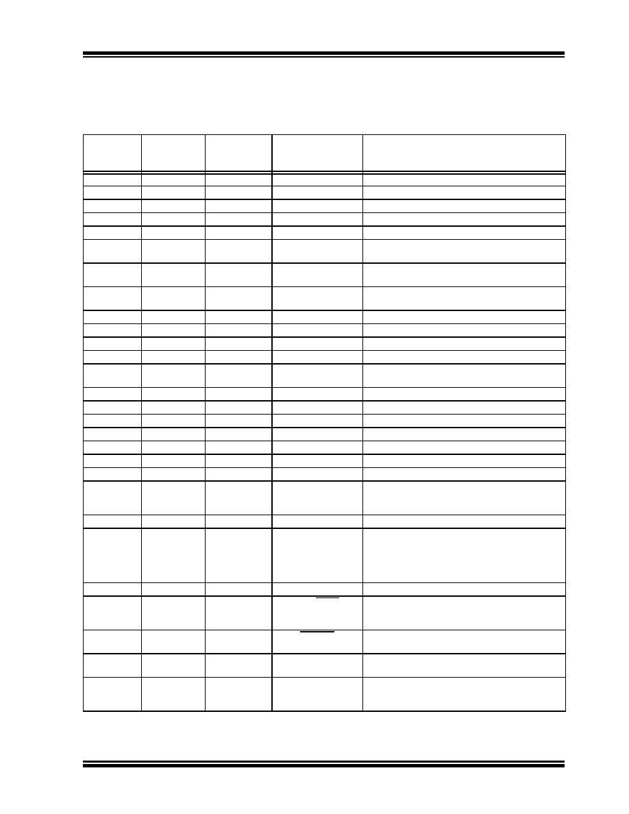
TABLE 2-1:
PIN FUNCTION TABLE
Pin Number
28-Pin PDIP,
28-Pin PLCC
Pin Number
44-Pin MQFP*
Pin Number
64-Pin MQFP*
Symbol
Description
1
39
10
V–
Negative power supply input.
2
40
11
REF IN
External reference input.
3
41
12
ANALOG COMMON
Reference point for REF IN.
4
2
18
INT OUT
Integrator output. Integrator capacitor connection.
5
3
20
AZ IN
Auto-zero inpt. Auto-zero capacitor connection.
6
4
22
BUFF OUT
Analog input buffer output. Integrator resistor
connection.
75
23
CREF–
Reference capacitor input. Reference capacitor
negative connection.
86
26
CREF+
Reference capacitor input. Reference capacitor
positive connection.
9
7
28
–INPUT
Analog input. Analog input negative connection.
10
8
30
+INPUT
Analog input. Analog input positive connection.
11
9
32
V+
Positive power supply input.
12
14
38
D5
Digit drive output. Most Significant Digit (MSD)
13
15
39
B1
Binary Coded Decimal (BCD) output. Least Significant
bit (LSb).
14
16
41
B2
BCD output.
15
17
42
B4
BCD output.
16
18
43
B8
BCD output. Most Significant bit (MSb).
17
19
44
D4
Digit drive output.
18
20
45
D3
Digit drive output.
19
25
52
D2
Digit drive output.
20
26
53
D1
Digit drive output. Least Significant Digit (LSD).
21
27
54
BUSY
Busy output. At the beginning of the signal-integration
phase, BUSY goes high and remains high until the
first clock pulse after the integrator zero crossing.
22
28
55
CLOCK IN
Clock input. Conversion clock connection.
23
29
57
POLARITY
Polarity output. A positive input is indicated by a logic
high output. The polarity output is valid at the
beginning of the reference integrate phase and
remains valid until determined during the next
conversion.
24
30
58
DGND
Digital logic reference input.
25
31
59
RUN/HOLD
Run/Hold input. When at a logic high, conversions are
performed continuously. A logic low holds the current
data as long as the low condition exists.
26
36
60
STROBE
Strobe output. The STROBE output pulses low in the
center of the digit drive outputs.
27
37
7
OVERRANGE
Overrange output. A logic high indicates that the
analog input exceeds the full-scale input range.
28
38
8
UNDERRANGE
Underrange output. A logic high indicates that the
analog input is less than 9% of the full-scale input
range.
*
Pins not identified or documented are NC (no connects).
相關PDF資料 |
PDF描述 |
|---|---|
| TC7135C/LI713 | 1-CH 4-BIT DUAL-SLOPE ADC, PARALLEL ACCESS, PQCC28 |
| TC7135C/KW | 1-CH 4-BIT DUAL-SLOPE ADC, PARALLEL ACCESS, PQFP44 |
| TC7135C/BU | 1-CH 4-BIT DUAL-SLOPE ADC, PARALLEL ACCESS, PQFP64 |
| TC7135CJI | DUAL-SLOPE ADC, PARALLEL ACCESS, CDIP28 |
| TC7135CLI | DUAL-SLOPE ADC, PARALLEL ACCESS, PQCC28 |
相關代理商/技術參數(shù) |
參數(shù)描述 |
|---|---|
| TC7135CLI713 | 功能描述:LED顯示驅動器 4-1/2 Digit A/D BCD RoHS:否 制造商:Micrel 數(shù)位數(shù)量:5 片段數(shù)量: 安裝風格:SMD/SMT 封裝 / 箱體:PLCC-44 工作電源電壓:4.75 V to 11 V 最大電源電流:10 mA 最大工作溫度:+ 85 C 最小工作溫度:- 40 C 封裝:Tube |
| TC7135CPI | 功能描述:LED顯示驅動器 4-1/2 Digit A/D BCD RoHS:否 制造商:Micrel 數(shù)位數(shù)量:5 片段數(shù)量: 安裝風格:SMD/SMT 封裝 / 箱體:PLCC-44 工作電源電壓:4.75 V to 11 V 最大電源電流:10 mA 最大工作溫度:+ 85 C 最小工作溫度:- 40 C 封裝:Tube |
| TC7135CPL | 制造商:MICROCHIP 制造商全稱:Microchip Technology 功能描述:4-1/2 Digit A/D Converter |
| TC7136 | 制造商:MICROCHIP 制造商全稱:Microchip Technology 功能描述:Low Power 3-1/2 Digit Analog-to-Digital Converter |
| TC7136A | 制造商:TELCOM 制造商全稱:TelCom Semiconductor, Inc 功能描述:LOW POWER, 3-1/2 DIGIT ANALOG-TO-DIGITAL CONVERTERS |
發(fā)布緊急采購,3分鐘左右您將得到回復。