- 您現在的位置:買賣IC網 > PDF目錄383931 > TC572502ECT (Microchip Technology Inc.) Line Regulator Controller PDF資料下載
參數資料
| 型號: | TC572502ECT |
| 廠商: | Microchip Technology Inc. |
| 英文描述: | Line Regulator Controller |
| 中文描述: | 線路穩(wěn)壓控制器 |
| 文件頁數: | 2/16頁 |
| 文件大?。?/td> | 462K |
| 代理商: | TC572502ECT |
TC57
DS21437B-page 2
2002 Microchip Technology Inc.
1.0
ELECTRICAL
CHARACTERISTICS
Absolute Maximum Ratings*
Input Voltage ........................................................+12V
Output Current ....................................................50mA
Output Voltage............................. -0.3V to (V
IN
+ 0.3V)
Power Dissipation.............................................150mW
Operating Temperature Range.............-40°C to +85°C
Storage Temperature Range..............-40°C to +150°C
*Stresses above those listed under "Absolute Maximum
Ratings" may cause permanent damage to the device. These
are stress ratings only and functional operation of the device
at these or any other conditions above those indicated in the
operation sections of the specifications is not implied.
Exposure to Absolute Maximum Rating conditions for
extended periods may affect device reliability.
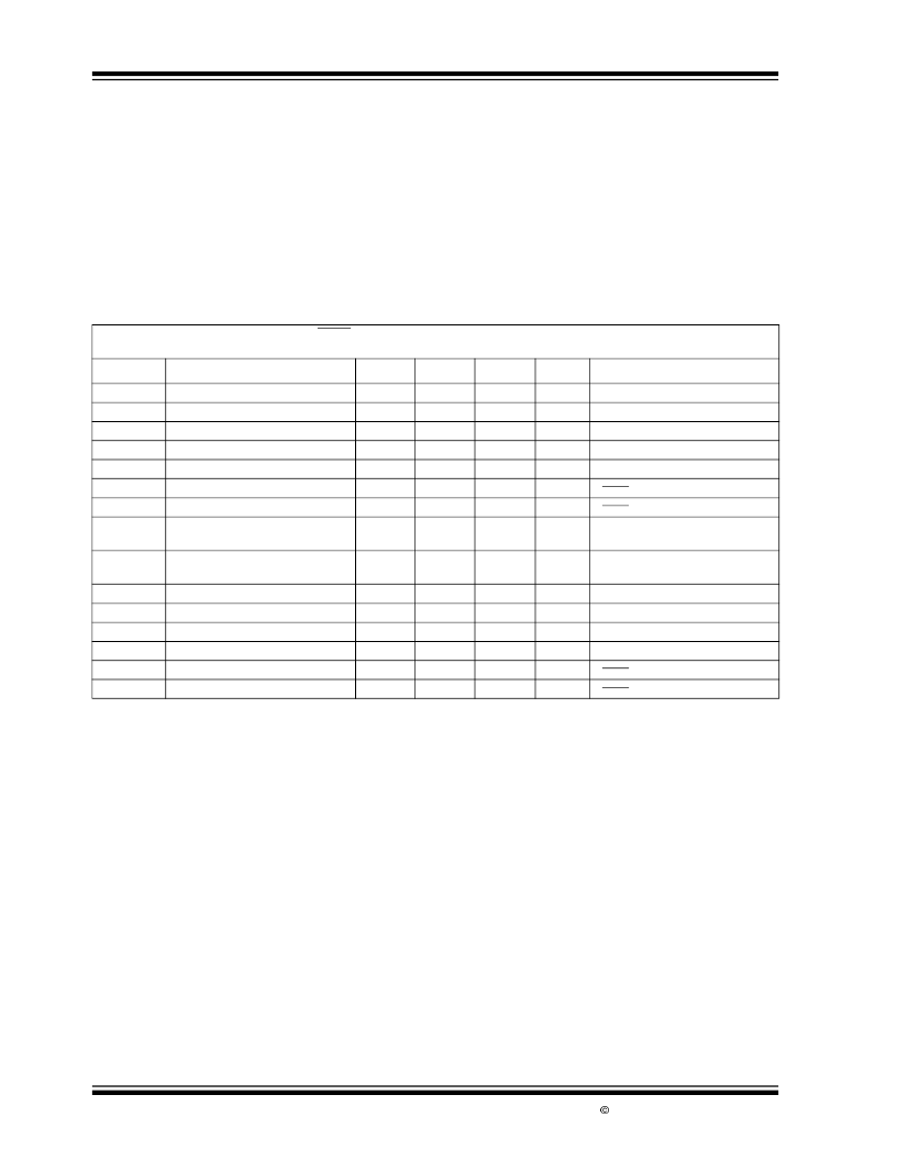
TC55 ELECTRICAL SPECIFICATIONS
TC57EP3002 Electrical Characteristics:
SHDN = GND, V
IN
= V
OUT
+ 1V, V
OUT
= 3V to 5V, I
OUT
= 0, T
A
= 25°C, Test Circuit of
Figure 3-1, unless otherwise noted.
(Note 2)
Symbol
Parameter
Min
Typ
Max
Units
Test Conditions
V
IN
V
EXT
V
OUT
V
OUT
V
IN
- V
OUT
I
DD
I
SHDN
V
OUT
/
V
IN
Input Voltage
Voltage on EXT Output
Output Voltage
Load Regulation
Dropout Voltage
Supply Current
Shutdown Supply Current
Line Regulation
—
—
—
—
8
8
V
V
V
0.98
X
V
R
V
R
±0.5% 1.02
X
V
R
-60
—
—
100
—
50
—
—
—
0.1
I
OUT
= 50mA
(Note 1)
1mA
≤
I
OUT
≤
100mA
(Note 3)
I
OUT
= 100mA
(Note 2)
V
SHDN
= V
IN
= 5V
V
SHDN
= GND
I
OUT
= 50mA, 4V
≤
V
IN
≤
8V
(Note 3
)
I
OUT
= 10mA, -40°C <
T
J
< +
85°C
(Note 3)
60
—
80
0.6
0.3
mV
mV
μ
A
μ
A
%/V
V
OUT
/
T
V
OUT
Temperature Coefficient
—
±100
—
ppm/°C
I
LEXT
I
EXT
V
IH
V
IL
I
IH
I
IL
Note
EXT Pin Leakage Current
EXT Sink Current
SHDN Input High Logic Threshold
SHDN Input Low Logic Threshold
SHDN Input Current @ V
IH
SHDN Input Current @ V
IL
V
is the regulator output voltage setting.
Dropout voltage is defined as the input to output differential at which the output voltage drops 2% below its nominal value measured at a
1V differential.
Varies with type of pass transistor used. Numbers shown are for the test circuit of Figure 3-1.
The product of I
EXTX
V
EXT
must be less than the maximum allowable power dissipation.
—
—
1.5
—
—
-0.2
—
—
—
—
—
0.5
25
—
0.25
0.1
0
μ
A
mA
V
V
μ
A
μ
A
Note 4
V
SHDN
= V
IN
= 5V
V
SHDN
= GND
-0.05
1:
2:
3:
4:
相關PDF資料 |
PDF描述 |
|---|---|
| TC573002ECT | Line Regulator Controller |
| TC573302ECT | Line Regulator Controller |
| TC573002 | Line Regulator Controller |
| TC573302 | Line Regulator Controller |
| TC593002ECB | Low Dropout, Negative Output Voltage Regulator |
相關代理商/技術參數 |
參數描述 |
|---|---|
| TC572502ECTTR | 功能描述:低壓差控制器 - LDO 2.5V Linear RoHS:否 制造商:Micrel 最大輸入電壓:5.5 V 輸出電壓:Adjustable 輸出電流:10 mA 負載調節(jié): 輸出類型:Adjustable, Fixed 輸出端數量:1 最大工作溫度:+ 125 C 安裝風格:SMD/SMT 封裝 / 箱體:SOT-23-6 |
| TC57256AD | 制造商:未知廠家 制造商全稱:未知廠家 功能描述:32,768 WORD x 8 BIT UV ERASABLE AND ELECTRICALLY PROGRAMMABLE READ ONLY MEMORY |
| TC57256AD-20 | 制造商:Toshiba America Electronic Components 功能描述: |
| TC57256D-25 | 制造商:TOSH. 85'S 功能描述:EPROM, 32K x 8, 28 Pin, Ceramic, DIP 制造商:Toshiba America Electronic Components 功能描述:EPROM, 32K x 8, 28 Pin, Ceramic, DIP |
| TC57256D-70 | 制造商:未知廠家 制造商全稱:未知廠家 功能描述:32,768 WORD x 8 BIT UV ERASABLE AND ELECTRICALLY PROGRAMMABLE READ ONLY MEMORY |
發(fā)布緊急采購,3分鐘左右您將得到回復。