- 您現在的位置:買賣IC網 > PDF目錄383928 > TC4420VOA713 (Microchip Technology Inc.) 6A High-Speed MOSFET Drivers PDF資料下載
參數資料
| 型號: | TC4420VOA713 |
| 廠商: | Microchip Technology Inc. |
| 英文描述: | 6A High-Speed MOSFET Drivers |
| 中文描述: | 6A條高速MOSFET驅動器 |
| 文件頁數: | 8/20頁 |
| 文件大小: | 280K |
| 代理商: | TC4420VOA713 |
TC4420/TC4429
DS21419C-page 8
2004 Microchip Technology Inc.
3.0
PIN DESCRIPTIONS
The descriptions of the pins are listed in Table 3-1.
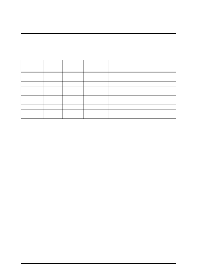
TABLE 3-1:
PIN FUNCTION TABLE
3.1
Supply Input (V
DD
)
The V
DD
input is the bias supply for the MOSFET driver
and is rated for 4.5V to 18V with respect to the ground
pins. The V
DD
input should be bypassed to ground with
a local ceramic capacitor. The value of the capacitor
should be chosen based on the capacitive load that is
being driven. A minimum value of 1.0 μF is suggested.
3.2
Control Input
The MOSFET driver input is a high-impedance,
TTL/CMOS compatible input. The input circuitry of the
TC4420/TC4429 MOSFET driver also has a “speed-
up” capacitor. This helps to decrease the propagation
delay times of the driver. Because of this, input signals
with slow rising or falling edges should not be used, as
this can result in double-pulsing of the MOSFET driver
output.
3.3
CMOS Push-Pull Output
The MOSFET driver output is a low-impedance,
CMOS, push-pull style output capable of driving a
capacitive load with 6.0A peak currents. The MOSFET
driver output is capable of withstanding 1.5A peak
reverse currents of either polarity.
3.4
Ground
The ground pins are the return path for the bias current
and the high peak currents that discharge the load
capacitor. The ground pins should be tied into a ground
plane or have very short traces to the bias supply
source return.
3.5
Exposed Metal Pad
The exposed metal pad of the 6x5 DFN package is not
internally connected to any potential. Therefore, this
pad can be connected to a ground plane or other
copper plane on a printed circuit board (PCB) to aid in
heat removal from the package.
Pin No.
8-Pin CERDIP/
PDIP/SOIC
Pin No.
8-Pin DFN
Pin No.
5-Pin TO-220
Symbol
Description
1
2
3
4
5
6
7
8
—
—
1
2
3
4
5
6
7
8
—
1
—
2
4
5
—
3
—
TAB
V
DD
INPUT
NC
GND
GND
OUTPUT
OUTPUT
V
DD
NC
V
DD
Supply input, 4.5V to 18V
Control input, TTL/CMOS compatible input
No Connection
Ground
Ground
CMOS push-pull output
CMOS push-pull output
Supply input, 4.5V to 18V
Exposed Metal Pad
Metal Tab is at the V
DD
Potential
PAD
—
相關PDF資料 |
PDF描述 |
|---|---|
| TC4420VPA | 6A High-Speed MOSFET Drivers |
| TC4420CG | 6A High-Speed MOSFET Drivers |
| TC4420CJA | 6A High-Speed MOSFET Drivers |
| TC4420CMF | 6A High-Speed MOSFET Drivers |
| TC4420CMF713 | 6A High-Speed MOSFET Drivers |
相關代理商/技術參數 |
參數描述 |
|---|---|
| TC4420VPA | 功能描述:功率驅動器IC 6A Sngl RoHS:否 制造商:Micrel 產品:MOSFET Gate Drivers 類型:Low Cost High or Low Side MOSFET Driver 上升時間: 下降時間: 電源電壓-最大:30 V 電源電壓-最小:2.75 V 電源電流: 最大功率耗散: 最大工作溫度:+ 85 C 安裝風格:SMD/SMT 封裝 / 箱體:SOIC-8 封裝:Tube |
| TC4421 | 制造商:MICROCHIP 制造商全稱:Microchip Technology 功能描述:9A High-Speed MOSFET Drivers |
| TC4421_04 | 制造商:MICROCHIP 制造商全稱:Microchip Technology 功能描述:9A High-Speed MOSFET Drivers |
| TC4421_13 | 制造商:MICROCHIP 制造商全稱:Microchip Technology 功能描述:9A High-Speed MOSFET Drivers |
| TC4421A | 制造商:MICROCHIP 制造商全稱:Microchip Technology 功能描述:9A High-Speed MOSFET Drivers |
發(fā)布緊急采購,3分鐘左右您將得到回復。