- 您現(xiàn)在的位置:買賣IC網(wǎng) > PDF目錄383928 > TC4420IAT (Microchip Technology Inc.) 6A High-Speed MOSFET Drivers PDF資料下載
參數(shù)資料
| 型號(hào): | TC4420IAT |
| 廠商: | Microchip Technology Inc. |
| 英文描述: | 6A High-Speed MOSFET Drivers |
| 中文描述: | 6A條高速M(fèi)OSFET驅(qū)動(dòng)器 |
| 文件頁數(shù): | 1/20頁 |
| 文件大小: | 280K |
| 代理商: | TC4420IAT |

2004 Microchip Technology Inc.
DS21419C-page 1
TC4420/TC4429
6A High-Speed MOSFET Drivers
Features
Latch-Up Protected: Will Withstand >1.5A
Reverse Output Current
Logic Input Will Withstand Negative Swing Up To
5V
ESD Protected: 4 kV
Matched Rise and Fall Times:
- 25 ns (2500 pF load)
High Peak Output Current: 6A
Wide Input Supply Voltage Operating Range:
- 4.5V to 18V
High Capacitive Load Drive Capability: 10,000 pF
Short Delay Time: 55 ns (typ.)
CMOS/TTL Compatible Input
Low Supply Current With Logic ‘
1
’ Input:
- 450 μA (typ.)
Low Output Impedance: 2.5
Output Voltage Swing to Within 25 mV of Ground
or V
DD
Space-Saving 8-Pin SOIC and 8-Pin 6x5 DFN
Packages
Applications
Switch-Mode Power Supplies
Motor Controls
Pulse Transformer Driver
Class D Switching Amplifiers
General Description
The TC4420/TC4429 are 6A (peak), single-output
MOSFET drivers. The TC4429 is an inverting driver
(pin-compatible with the TC429), while the TC4420 is a
non-inverting driver. These drivers are fabricated in
CMOS for lower power and more efficient operation
versus bipolar drivers.
Both devices have TTL/CMOS compatible inputs that
can be driven as high as V
DD
+ 0.3V or as low as –5V
without upset or damage to the device. This eliminates
the need for external level-shifting circuitry and its
associated cost and size. The output swing is rail-to-rail,
ensuring better drive voltage margin, especially during
power-up/power-down
sequencing.
delay time is only 55 ns (typ.) and the output rise and fall
times are only 25 ns (typ.) into 2500 pF across the
usable power supply range.
Unlike other drivers, the TC4420/TC4429 are virtually
latch-up proof. They replace three or more discrete
components, saving PCB area, parts and improving
overall system reliability.
Propagational
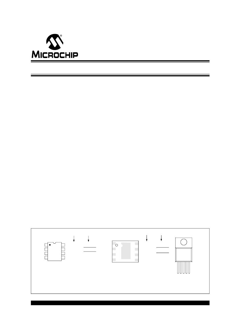
Package Types
(1)
5-Pin TO-220
V
D
G
I
G
O
TC4420
TC4429
Tab is
Common
to V
DD
8-Pin CERDIP/
PDIP/SOIC
1
2
3
4
V
DD
OUTPUT
OUTPUT
5
6
7
8
GND
V
DD
INPUT
NC
GND
TC4420
TC4429
TC4420
TC4429
V
DD
OUTPUT
OUTPUT
GND
Note 1:
Duplicate pins must both be connected for proper operation.
Exposed pad of the DFN package is electrically isolated.
2:
8-Pin DFN
(2)
V
DD
INPUT
NC
GND
2
3
4
5
6
7
8
1
TC4420
TC4429
V
DD
OUTPUT
GND
OUTPUT
TC4420 TC4429
V
DD
OUTPUT
GND
OUTPUT
相關(guān)PDF資料 |
PDF描述 |
|---|---|
| TC4420IG | 6A High-Speed MOSFET Drivers |
| TC4420IMF | 6A High-Speed MOSFET Drivers |
| TC4421CG | 9A High-Speed MOSFET Drivers |
| TC4421CMF | 9A High-Speed MOSFET Drivers |
| TC4421CMF713 | 9A High-Speed MOSFET Drivers |
相關(guān)代理商/技術(shù)參數(shù) |
參數(shù)描述 |
|---|---|
| TC4420IG | 制造商:MICROCHIP 制造商全稱:Microchip Technology 功能描述:6A High-Speed MOSFET Drivers |
| TC4420IJA | 功能描述:功率驅(qū)動(dòng)器IC 6A Sngl RoHS:否 制造商:Micrel 產(chǎn)品:MOSFET Gate Drivers 類型:Low Cost High or Low Side MOSFET Driver 上升時(shí)間: 下降時(shí)間: 電源電壓-最大:30 V 電源電壓-最小:2.75 V 電源電流: 最大功率耗散: 最大工作溫度:+ 85 C 安裝風(fēng)格:SMD/SMT 封裝 / 箱體:SOIC-8 封裝:Tube |
| TC4420IMF | 制造商:MICROCHIP 制造商全稱:Microchip Technology 功能描述:6A High-Speed MOSFET Drivers |
| TC4420IMF713 | 制造商:MICROCHIP 制造商全稱:Microchip Technology 功能描述:6A High-Speed MOSFET Drivers |
| TC4420IOA | 制造商:MICROCHIP 制造商全稱:Microchip Technology 功能描述:6A High-Speed MOSFET Drivers |
發(fā)布緊急采購,3分鐘左右您將得到回復(fù)。