- 您現(xiàn)在的位置:買賣IC網(wǎng) > PDF目錄383927 > TC2117-2.5DBTR (Microchip Technology Inc.) 800 mA Fixed Low Dropout Positive Regulator PDF資料下載
參數(shù)資料
| 型號(hào): | TC2117-2.5DBTR |
| 廠商: | Microchip Technology Inc. |
| 英文描述: | 800 mA Fixed Low Dropout Positive Regulator |
| 中文描述: | 800毫安固定低壓差穩(wěn)壓器正 |
| 文件頁數(shù): | 2/18頁 |
| 文件大?。?/td> | 751K |
| 代理商: | TC2117-2.5DBTR |
TC2117
DS21665C-page 2
2006 Microchip Technology Inc.
1.0
ELECTRICAL
CHARACTERISTICS
Absolute Maximum Ratings
Input Voltage .........................................................6.5V
Output Voltage.................... (V
SS
– 0.3) to (V
IN
+ 0.3V)
Power Dissipation................Internally Limited
(Note 7)
Maximum Voltage on Any Pin .........V
IN
+0.3V to -0.3V
Operating Temperature ...............-40°C < T
J
< +125°C
Storage temperature ..........................-65°C to +150°C
Notice:
Stresses above those listed under "Absolute Maxi-
mum Ratings" may cause permanent damage to the device.
These are stress ratings only and functional operation of the
device at these or any other conditions above those indicated
in the operation sections of the specifications is not implied.
Exposure to Absolute Maximum Rating conditions for
extended periods may affect device reliability.
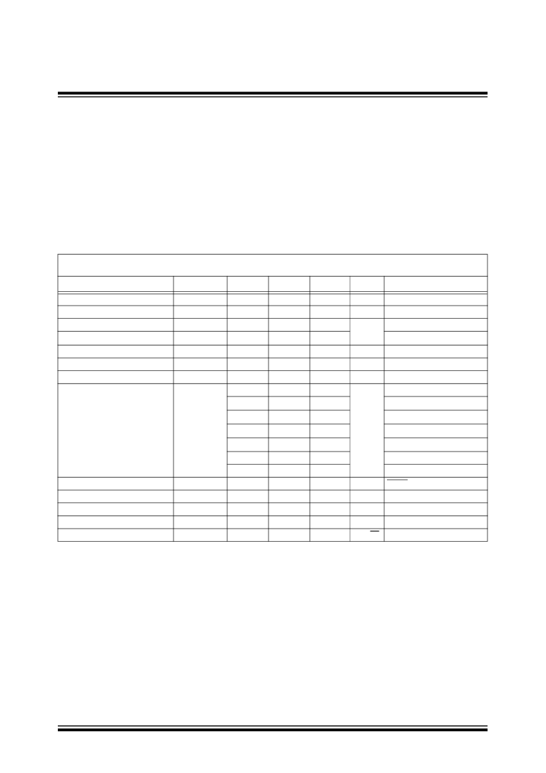
DC CHARACTERISTICS
Electrical Specifications:
Unless otherwise indicated, V
IN
= V
R
+ 1.5V,
(Note 1)
, I
L
= 100 μA, C
L
= 3.3 μF, T
A
= +25°C.
Boldface
type specifications apply for junction temperatures of -40°C to +125°C.
Parameters
Sym
Min
Typ
Max
Units
Conditions
Input Operating Voltage
V
IN
2.7
—
6.0
V
Note 2
Maximum Output Current
I
OUTMAX
V
OUT
800
—
—
mA
Output Voltage
V
R
– 2.5%
V
R
– 2%
V
R
± 0.5%
V
R
+ 2.5%
V
R
± 0.5%
V
V
R
≥
2.5V
V
R
= 1.8V
V
R
+ 3%
V
OUT
Temperature Coefficient
Line Regulation
Δ
V
OUT
/
Δ
T
Δ
V
OUT
/
Δ
V
IN
Δ
V
OUT
/V
OUT
V
IN
–V
OUT
—
40
—
ppm/°C
Note 3
—
0.007
0.35
%
(V
R
+ 1V)
≤
V
IN
≤
6V
I
L
= 0.1 mA to I
OUTMAX
V
R
≥
2.5V, I
L
= 100 μA
V
R
≥
2.5V,
I
L
=
100
mA
V
R
≥
2.5V,
I
L
= 300 mA
V
R
≥
2.5V,
I
L
= 500 mA
V
R
≥
2.5V,
I
L
= 800 mA
V
R
= 1.8V, I
L
= 500 mA
I
L
= 800 mA
SHDN = V
IH
, I
L
= 0
F
≤
1 kHz
Load Regulation
(Note 4)
-0.01
0.002
0
%/mA
Dropout Voltage
(Note 5)
—
20
30
mV
—
50
160
—
150
480
—
260
800
—
450
1300
—
1000
1200
—
1200
1400
Supply Current
I
DD
PSRR
—
80
130
μA
Power Supply Rejection Ratio
—
55
—
db
Output Short Circuit Current
I
OUTSC
Δ
V
OUT
/
Δ
P
D
eN
—
1200
—
mA
V
OUT
= 0V
Note 6
Thermal Regulation
—
0.04
—
V/W
Output Noise
—
300
—
nV/
√
Hz
I
L
= 100 mA, F = 10 kH
Z
Note
1:
2:
3:
V
R
is the regulator output voltage setting.
The minimum V
IN
has to justify the conditions: V
IN
≥
V
R
+ V
DROPOUT
and V
IN
≥
2.7V for I
L
= 0.1 mA to I
OUTMAX
.
(
)
10
6
–
V
OUT
T
4:
Regulation is measured at a constant junction temperature using low duty cycle pulse testing. Load regulation is tested
over a load range from 0.1 mA to the maximum specified output current. Changes in output voltage due to heating
effects are covered by the thermal regulation specification.
Dropout voltage is defined as the input-to-output differential at which the output voltage drops 2% below its nominal
value measured at a 1.5V differential.
Thermal regulation is defined as the change in output voltage at a time T after a change in power dissipation is applied,
excluding load or line regulation effects. Specifications are for a current pulse equal to I
LMAX
at V
IN
= 6V for T = 10 ms.
The maximum allowable power dissipation is a function of ambient temperature, the maximum allowable junction tem-
perature and the thermal resistance from junction-to-air (i.e., T
A
, T
J
,
θ
JA
). Exceeding the maximum allowable power dis-
sipation causes the device to initiate thermal shutdown. Please see
Section 4.2 “Thermal Considerations”
for more
details.
5:
6:
7:
TCV
OUT
OUTMAX
-V
V
OUTMIN
–
=
相關(guān)PDF資料 |
PDF描述 |
|---|---|
| TC2117-2.5EB | 800 mA Fixed Low Dropout Positive Regulator |
| TC2117-2.5EDTR | 800 mA Fixed Low Dropout Positive Regulator |
| TC2117-3.0DB | 800 mA Fixed Low Dropout Positive Regulator |
| TC2117-3.0DBTR | 800 mA Fixed Low Dropout Positive Regulator |
| TC2117-3.0EB | 800 mA Fixed Low Dropout Positive Regulator |
相關(guān)代理商/技術(shù)參數(shù) |
參數(shù)描述 |
|---|---|
| TC2117-3.0DB | 制造商:MICROCHIP 制造商全稱:Microchip Technology 功能描述:800 mA Fixed Low Dropout Positive Regulator |
| TC2117-3.0DBTR | 制造商:MICROCHIP 制造商全稱:Microchip Technology 功能描述:800 mA Fixed Low Dropout Positive Regulator |
| TC2117-3.0EB | 制造商:MICROCHIP 制造商全稱:Microchip Technology 功能描述:800 mA Fixed Low Dropout Positive Regulator |
| TC2117-3.0EDTR | 制造商:MICROCHIP 制造商全稱:Microchip Technology 功能描述:800 mA Fixed Low Dropout Positive Regulator |
| TC2117-3.0VDBTR | 功能描述:低壓差穩(wěn)壓器 - LDO 800mA Fixed Output RoHS:否 制造商:Texas Instruments 最大輸入電壓:36 V 輸出電壓:1.4 V to 20.5 V 回動(dòng)電壓(最大值):307 mV 輸出電流:1 A 負(fù)載調(diào)節(jié):0.3 % 輸出端數(shù)量: 輸出類型:Fixed 最大工作溫度:+ 125 C 安裝風(fēng)格:SMD/SMT 封裝 / 箱體:VQFN-20 |
發(fā)布緊急采購(gòu),3分鐘左右您將得到回復(fù)。