- 您現(xiàn)在的位置:買賣IC網(wǎng) > PDF目錄383901 > TC1303B-EJ3EUNTR (Microchip Technology Inc.) 500 mA Synchronous Buck Regulator, + 300 mA LDO with Power-Good Output PDF資料下載
參數(shù)資料
| 型號: | TC1303B-EJ3EUNTR |
| 廠商: | Microchip Technology Inc. |
| 英文描述: | 500 mA Synchronous Buck Regulator, + 300 mA LDO with Power-Good Output |
| 中文描述: | 500毫安同步降壓穩(wěn)壓器,300 mA的LDO具有電源就緒輸出 |
| 文件頁數(shù): | 15/30頁 |
| 文件大?。?/td> | 441K |
| 代理商: | TC1303B-EJ3EUNTR |
第1頁第2頁第3頁第4頁第5頁第6頁第7頁第8頁第9頁第10頁第11頁第12頁第13頁第14頁當前第15頁第16頁第17頁第18頁第19頁第20頁第21頁第22頁第23頁第24頁第25頁第26頁第27頁第28頁第29頁第30頁
2005 Microchip Technology Inc.
DS21949A-page 15
TC1303B
3.0
PIN DESCRIPTIONS
The descriptions of the pins are listed in Table 3-1.
TABLE 3-1:
PIN FUNCTION TABLE
3.1
LDO Shutdown Input Pin (SHDN2)
SHDN2 is a logic level input used to turn the LDO Reg-
ulator on and off. A logic high (> 45% of V
IN
), will enable
the regulator output. A logic low (< 15% of V
IN
) will
ensure that the output is turned off.
3.2
LDO Input Voltage Pin (V
IN2
)
V
IN2
is a LDO power input supply pin. Connect variable
input voltage source to V
IN2
.
Connect V
IN1
and V
IN2
together with board traces as short as possible. V
IN2
provides the input voltage for the LDO regulator. An
additional capacitor can be added to lower the LDO
regulator input ripple voltage.
3.3
LDO Output Voltage Pin (V
OUT2
)
V
OUT2
is a regulated LDO output voltage pin. Connect
a 1 μF or larger capacitor to V
OUT2
and A
GND
for proper
operation.
3.4
Power-Good Output Pin (PG)
PG is an output level indicating that V
OUT2
(LDO) is
within 94% of regulation. The PG output is configured
as a push-pull for the TC1303B.
3.5
Analog Ground Pin (A
GND
)
A
GND
is the analog ground connection. Tie A
GND
to the
analog portion of the ground plane (A
GND
). See the
physical layout information in
Section 5.0 “Application
Circuits/Issues”
for grounding recommendations.
3.6
Buck Regulator Output Sense Pin
(V
FB
/V
OUT1
)
For V
OUT1
adjustable output voltage options, connect
the center of the output voltage divider to the V
FB
pin.
For fixed-output voltage options, connect the output of
the buck regulator to this pin (V
OUT1
).
3.7
Buck Regulator Shutdown Input
Pin (SHDN1)
SHDN1 is a logic level input used to turn the buck
regulator on and off. A logic-high (> 45% of V
IN
), will
enable the regulator output. A logic-low (< 15% of V
IN
)
will ensure that the output is turned off.
3.8
Buck Regulator Input Voltage Pin
(V
IN1
)
V
IN1
is the buck regulator power input supply pin.
Connect a variable input voltage source to V
IN1
.
Connect V
IN1
and V
IN2
together with board traces as
short as possible.
3.9
Buck Inductor Output Pin (L
X
)
Connect L
X
directly to the buck inductor. This pin
carries large signal-level current; all connections
should be made as short as possible.
3.10
Power Ground Pin (P
GND
)
Connect all large-signal level ground returns to P
GND
.
These large-signal, level ground traces should have a
small loop area and length to prevent coupling of
switching noise to sensitive traces. Please see the
physical layout information supplied in
Section 5.0
“Application
Circuits/Issues”
recommendations.
3.11
Exposed Pad (EP)
For the DFN package, connect the EP to A
GND
with
vias into the A
GND
plane.
for
grounding
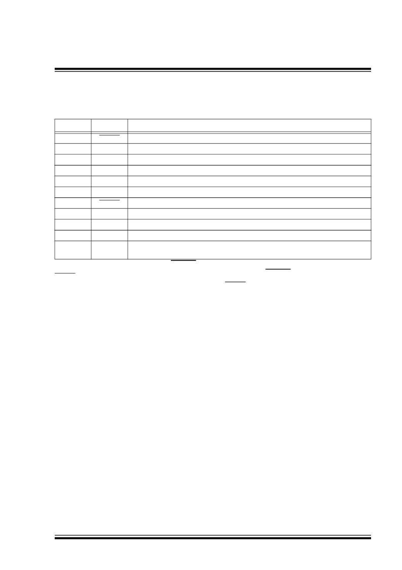
Pin No.
Name
Function
1
SHDN2
Active Low Shutdown Input for LDO Output Pin
2
V
IN2
V
OUT2
PG
Analog Input Supply Voltage Pin
3
LDO Output Voltage Pin
4
Power-good Output Pin
5
A
GND
Analog Ground Pin
6
V
FB
/ V
OUT1
Buck Feedback Voltage (Adjustable Version) / Buck Output Voltage (Fixed Version) Pin
SHDN1
Active Low Shutdown Input for Buck Regulator Output Pin
7
8
V
IN1
L
X
P
GND
Exposed
Pad
Buck Regulator Input Voltage Pin
9
Buck Inductor Output Pin
10
Power Ground Pin
EP
For the DFN package, the center exposed pad is a thermal path to remove heat from the
device. Electrically this pad is at ground potential and should be connected to A
GND
.
相關PDF資料 |
PDF描述 |
|---|---|
| TC1303B-EK0EMF | 500 mA Synchronous Buck Regulator, + 300 mA LDO with Power-Good Output |
| TC1303B-EK0EMFTR | 500 mA Synchronous Buck Regulator, + 300 mA LDO with Power-Good Output |
| TC1303B-EK0EUN | 500 mA Synchronous Buck Regulator, + 300 mA LDO with Power-Good Output |
| TC1303B-EK0EUNTR | 500 mA Synchronous Buck Regulator, + 300 mA LDO with Power-Good Output |
| TC1303B-EK1EMF | 500 mA Synchronous Buck Regulator, + 300 mA LDO with Power-Good Output |
相關代理商/技術參數(shù) |
參數(shù)描述 |
|---|---|
| TC1303B-IA0EMF | 功能描述:低壓差穩(wěn)壓器 - LDO PWM/LDO combo w/PG RoHS:否 制造商:Texas Instruments 最大輸入電壓:36 V 輸出電壓:1.4 V to 20.5 V 回動電壓(最大值):307 mV 輸出電流:1 A 負載調(diào)節(jié):0.3 % 輸出端數(shù)量: 輸出類型:Fixed 最大工作溫度:+ 125 C 安裝風格:SMD/SMT 封裝 / 箱體:VQFN-20 |
| TC1303B-IA0EMFTR | 功能描述:低壓差穩(wěn)壓器 - LDO PWM/LDO combo w/PG RoHS:否 制造商:Texas Instruments 最大輸入電壓:36 V 輸出電壓:1.4 V to 20.5 V 回動電壓(最大值):307 mV 輸出電流:1 A 負載調(diào)節(jié):0.3 % 輸出端數(shù)量: 輸出類型:Fixed 最大工作溫度:+ 125 C 安裝風格:SMD/SMT 封裝 / 箱體:VQFN-20 |
| TC1303B-IA0EUN | 功能描述:低壓差穩(wěn)壓器 - LDO PWM/LDO combo w/PG RoHS:否 制造商:Texas Instruments 最大輸入電壓:36 V 輸出電壓:1.4 V to 20.5 V 回動電壓(最大值):307 mV 輸出電流:1 A 負載調(diào)節(jié):0.3 % 輸出端數(shù)量: 輸出類型:Fixed 最大工作溫度:+ 125 C 安裝風格:SMD/SMT 封裝 / 箱體:VQFN-20 |
| TC1303B-IA0EUNTR | 功能描述:低壓差穩(wěn)壓器 - LDO PWM/LDO combo w/PG RoHS:否 制造商:Texas Instruments 最大輸入電壓:36 V 輸出電壓:1.4 V to 20.5 V 回動電壓(最大值):307 mV 輸出電流:1 A 負載調(diào)節(jié):0.3 % 輸出端數(shù)量: 輸出類型:Fixed 最大工作溫度:+ 125 C 安裝風格:SMD/SMT 封裝 / 箱體:VQFN-20 |
| TC1303B-PA0EMF | 功能描述:低壓差穩(wěn)壓器 - LDO PWM/LDO combo w/PG RoHS:否 制造商:Texas Instruments 最大輸入電壓:36 V 輸出電壓:1.4 V to 20.5 V 回動電壓(最大值):307 mV 輸出電流:1 A 負載調(diào)節(jié):0.3 % 輸出端數(shù)量: 輸出類型:Fixed 最大工作溫度:+ 125 C 安裝風格:SMD/SMT 封裝 / 箱體:VQFN-20 |
發(fā)布緊急采購,3分鐘左右您將得到回復。