- 您現(xiàn)在的位置:買賣IC網(wǎng) > PDF目錄359287 > TC1264-3.0VDBRT 3 V FIXED POSITIVE LDO REGULATOR, 1.3 V DROPOUT, PSSO3 PDF資料下載
參數(shù)資料
| 型號: | TC1264-3.0VDBRT |
| 元件分類: | 固定正電壓單路輸出LDO穩(wěn)壓器 |
| 英文描述: | 3 V FIXED POSITIVE LDO REGULATOR, 1.3 V DROPOUT, PSSO3 |
| 封裝: | SOT-223, 3 PIN |
| 文件頁數(shù): | 2/8頁 |
| 文件大小: | 55K |
| 代理商: | TC1264-3.0VDBRT |
2
TC1264
800mA Fixed Output CMOS LDO
TC1264-4 3/28/00
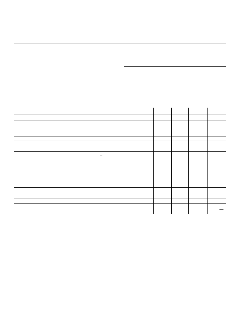
ELECTRICAL CHARACTERISTICS:
V
IN
= V
R
+ 1.5V
(Note 1)
, I
L
= 100
μ
A, C
L
= 3.3
μ
F, T
A
= 25
°
C, unless otherwise
specified.
BOLDFACE
type specifications apply for junction temperatures of –
40
°
C to +125
°
C.
Symbol
Parameter
Test Conditions
Min
Typ
Max
Units
V
IN
I
OUTMAX
V
OUT
Input Operating Voltage
Maximum Output Current
Output Voltage
(Note 2)
2.7
800
—
—
6.0
—
V
mA
V
V
R
> 2.5V
V
R
= 1.8V
Note 3
(V
R
+ 1V) < V
IN
< 6V
I
L
= 0.1mA to I
OUTMAX
(Note 4)
V
R
> 2.5V, I
L
= 100
μ
A
I
L
= 100mA
I
L
= 300mA
I
L
= 500mA
I
L
= 800mA
V
R
= 1.8V, I
L
= 500mA
I
L
= 800mA
(Note 5)
I
L
= 0
F
≤
1kHz
V
OUT
= 0V
Note 6
I
L
= I
OUTMAX
, F = 10kHz
V
R
– 2.5%
V
R
±
0.5%
V
R
+ 2.5%
V
R
– 2%
V
R
±
0.5%
—
40
—
0.007
-0.01
0.002
—
20
—
50
—
150
—
260
—
450
—
700
—
890
V
R
+ 3%
—
0.35
0
30
160
480
800
1300
1000
1400
V
OUT
/
T
V
OUT
/
V
IN
V
OUT
/V
OUT
V
IN
– V
OUT
V
OUT
Temperature Coefficient
Line Regulation
Load Regulation
Dropout Voltage
ppm/
°
C
%
%/mA
mV
I
DD
PSRR
I
OUTSC
V
OUT
/
P
D
eN
NOTES:
1. V
R
is the regulator output voltage setting.
2. The minimum V
IN
has to justify the conditions: V
IN
> V
R
+ V
DROPOUT
and V
IN
> 2.7V for I
L
= 0.1mA to I
OUTMAX
.
3. T
C
V
OUT
= (V
OUTMAX
–
V
OUTMIN
)
x 10
V
OUT
x
T
4. Regulation is measured at a constant junction temperature using low duty cycle pulse testing. Load regulation is tested over a load
range from 0.1mA to the maximum specified output current. Changes in output voltage due to heating effects are covered by the thermal
regulation specification.
5. Dropout voltage is defined as the input to output differential at which the output voltage drops 2% below its nominal value measured at a
1.5V differential.
6. Thermal Regulation is defined as the change in output voltage at a time T after a change in power dissipation is applied, excluding load
or line regulation effects. Specifications are for a current pulse equal to I
LMAX
at V
IN
= 6V for T = 10msec.
7. The maximum allowable power dissipation is a function of ambient temperature, the maximum allowable junction temperature, and the
thermal resistance from junction-to-air (i.e. T
A
, T
J
,
θ
JA
). Exceeding the maximum allowable power dissipation causes the device to
initiate thermal shutdown. Please see
Thermal Considerations
section of this data sheet for more details.
Supply Current
Power Supply Rejection Ratio
Output Short Circuit Current
Thermal Regulation
Output Noise
—
—
—
—
—
80
64
1200
0.04
260
130
—
—
—
—
A
dB
mA
V/W
nV/
√
Hz
ABSOLUTE MAXIMUM RATINGS*
Input Voltage ..............................................................6.5V
Output Voltage ........................... (V
SS
– 0.3) to (V
IN
+ 0.3)
Power Dissipation ....................Internally Limited (Note 7)
Operating Temperature.................... – 40
°
C < T
J
< 125
°
C
Storage Temperature ............................– 65
°
C to +150
°
C
Maximum Voltage on Any Pin ........... V
IN
+ 0.3V to – 0.3V
Lead Temperature (Soldering, 10 Sec.)................+260
°
C
*Absolute Maximum Ratings indicate device operation limits beyond dam-
age may occur. Device operation beyond the limits listed in Electrical
Characteristics is not recommended.
相關(guān)PDF資料 |
PDF描述 |
|---|---|
| TC1264-3.0VDBTR | 3 V FIXED POSITIVE LDO REGULATOR, 1.3 V DROPOUT, PSSO3 |
| TC1264-3.0VEBTR | 3 V FIXED POSITIVE LDO REGULATOR, 1.3 V DROPOUT, PSSO3 |
| TC1264-3.3VAB | 3.3 V FIXED POSITIVE LDO REGULATOR, 1.3 V DROPOUT, PSFM3 |
| TC1264-3.3VDBTR | 3.3 V FIXED POSITIVE LDO REGULATOR, 1.3 V DROPOUT, PSSO3 |
| TC1264-3.3VDB | 3.3 V FIXED POSITIVE LDO REGULATOR, 1.3 V DROPOUT, PSSO3 |
相關(guān)代理商/技術(shù)參數(shù) |
參數(shù)描述 |
|---|---|
| TC126433VAB | 制造商:TELCOM 功能描述:* |
| TC1265 | 功能描述:鋁質(zhì)電解電容器 - 帶引線 100uF 250V RoHS:否 制造商:Kemet 引線類型: 電容:220 uF 容差:20 % 電壓額定值:25 V 工作溫度范圍: 端接類型:Radial 外殼直徑:8 mm 外殼長度:11 mm 引線間隔:5 mm 產(chǎn)品:General Purpose Electrolytic Capacitors 封裝:Bulk |
| TC1265_06 | 制造商:MICROCHIP 制造商全稱:Microchip Technology 功能描述:800 mA Fixed-Output CMOS LDO with Shutdown |
| TC126501ECTTR | 功能描述:開關(guān)變換器、穩(wěn)壓器與控制器 PFM Step-up DC/DC RoHS:否 制造商:Texas Instruments 輸出電壓:1.2 V to 10 V 輸出電流:300 mA 輸出功率: 輸入電壓:3 V to 17 V 開關(guān)頻率:1 MHz 工作溫度范圍: 安裝風(fēng)格:SMD/SMT 封裝 / 箱體:WSON-8 封裝:Reel |
| TC126503ECT | 制造商:MICROCHIP 制造商全稱:Microchip Technology 功能描述:PFM Step-Up DC/DC Regulators |
發(fā)布緊急采購,3分鐘左右您將得到回復(fù)。