- 您現(xiàn)在的位置:買(mǎi)賣(mài)IC網(wǎng) > PDF目錄98166 > TB2902HQ 45 W, 4 CHANNEL, AUDIO AMPLIFIER, PZFM25 PDF資料下載
參數(shù)資料
| 型號(hào): | TB2902HQ |
| 元件分類(lèi): | 音頻/視頻放大 |
| 英文描述: | 45 W, 4 CHANNEL, AUDIO AMPLIFIER, PZFM25 |
| 封裝: | 1 MM PITCH, PLASTIC, HZIP-25 |
| 文件頁(yè)數(shù): | 12/38頁(yè) |
| 文件大?。?/td> | 444K |
| 代理商: | TB2902HQ |
第1頁(yè)第2頁(yè)第3頁(yè)第4頁(yè)第5頁(yè)第6頁(yè)第7頁(yè)第8頁(yè)第9頁(yè)第10頁(yè)第11頁(yè)當(dāng)前第12頁(yè)第13頁(yè)第14頁(yè)第15頁(yè)第16頁(yè)第17頁(yè)第18頁(yè)第19頁(yè)第20頁(yè)第21頁(yè)第22頁(yè)第23頁(yè)第24頁(yè)第25頁(yè)第26頁(yè)第27頁(yè)第28頁(yè)第29頁(yè)第30頁(yè)第31頁(yè)第32頁(yè)第33頁(yè)第34頁(yè)第35頁(yè)第36頁(yè)第37頁(yè)第38頁(yè)
TB2902HQ
2004-08-18
2
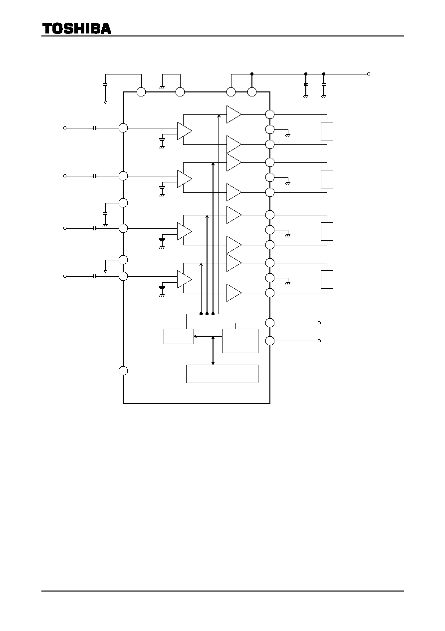
Block Diagram
Some of the functional blocks, circuits, or constants labels in the block diagram may have been omitted or
simplified for clarity.
11
Ripple
IN1
9
Out1 (
+)
10
TAB
1
VCC2
6
VCC1
20
C5
C3
C2
8
7
C1
R
L
=4
PW-GND1
Out1 (
)
+B
12
IN2
5
Out2 (
+)
2
3
C1
R
L
=4
PW-GND2
Out2 (
)
15
IN3
17
Out3 (
+)
18
19
C1
R
L
=4
PW-GND3
Out3 (
)
14
IN4
21
Out4 (
+)
24
23
C1
R
L
=4
PW-GND4
Out4 (
)
C4
16
For Mute
Time constant
13 Pre-GND
4
Clip Detection
22
25
SCL
SDA
SW
I
2C
Bus
Diagnosis
RF
RR
LF
LR
相關(guān)PDF資料 |
PDF描述 |
|---|---|
| TB2903HQ | 29 W, 4 CHANNEL, AUDIO AMPLIFIER, PZFM25 |
| TB2903HQ | 29 W, 4 CHANNEL, AUDIO AMPLIFIER, PZFM25 |
| TB2904HQ | 26 W, 4 CHANNEL, AUDIO AMPLIFIER, PZFM25 |
| TB2904HQ | 26 W, 4 CHANNEL, AUDIO AMPLIFIER, PZFM25 |
| TB2905HQ | 55 W, 4 CHANNEL, AUDIO AMPLIFIER, PZFM25 |
相關(guān)代理商/技術(shù)參數(shù) |
參數(shù)描述 |
|---|---|
| TB2903HQ | 制造商:TOSHIBA 制造商全稱(chēng):Toshiba Semiconductor 功能描述:Maximum Power 47W BTL x 4-ch Audio Power IC |
| TB2904HQ | 制造商:TOSHIBA 制造商全稱(chēng):Toshiba Semiconductor 功能描述:Maximum Power 43 W BTL ?4-ch Audio Power IC |
| TB2905HQ | 制造商:TOSHIBA 制造商全稱(chēng):Toshiba Semiconductor 功能描述:Class KB High-Efficiency, Low-Frequency Power Amplifier IC Maximum Power: 47 W x 4 Channels |
| TB2905HQ(O) | 功能描述:音頻放大器 25W x 4ch Class-KB Car Pwr Amp RoHS:否 制造商:STMicroelectronics 產(chǎn)品:General Purpose Audio Amplifiers 輸出類(lèi)型:Digital 輸出功率: THD + 噪聲: 工作電源電壓:3.3 V 電源電流: 最大功率耗散: 最大工作溫度: 安裝風(fēng)格:SMD/SMT 封裝 / 箱體:TQFP-64 封裝:Reel |
| TB2906HQ | 制造商:TOSHIBA 制造商全稱(chēng):Toshiba Semiconductor 功能描述:Maximum Power 43 W BTL x 4-ch Audio Power IC |
發(fā)布緊急采購(gòu),3分鐘左右您將得到回復(fù)。