- 您現(xiàn)在的位置:買賣IC網(wǎng) > PDF目錄98165 > TAS5710PHP (TEXAS INSTRUMENTS INC) 20.2 W, 2 CHANNEL, AUDIO AMPLIFIER, PQFP48 PDF資料下載
參數(shù)資料
| 型號: | TAS5710PHP |
| 廠商: | TEXAS INSTRUMENTS INC |
| 元件分類: | 音頻/視頻放大 |
| 英文描述: | 20.2 W, 2 CHANNEL, AUDIO AMPLIFIER, PQFP48 |
| 封裝: | 7 X 7 MM, GREEN, PLASTIC, HTQFP-64 |
| 文件頁數(shù): | 21/57頁 |
| 文件大小: | 1124K |
| 代理商: | TAS5710PHP |
第1頁第2頁第3頁第4頁第5頁第6頁第7頁第8頁第9頁第10頁第11頁第12頁第13頁第14頁第15頁第16頁第17頁第18頁第19頁第20頁當前第21頁第22頁第23頁第24頁第25頁第26頁第27頁第28頁第29頁第30頁第31頁第32頁第33頁第34頁第35頁第36頁第37頁第38頁第39頁第40頁第41頁第42頁第43頁第44頁第45頁第46頁第47頁第48頁第49頁第50頁第51頁第52頁第53頁第54頁第55頁第56頁第57頁

BANK SWITCHING
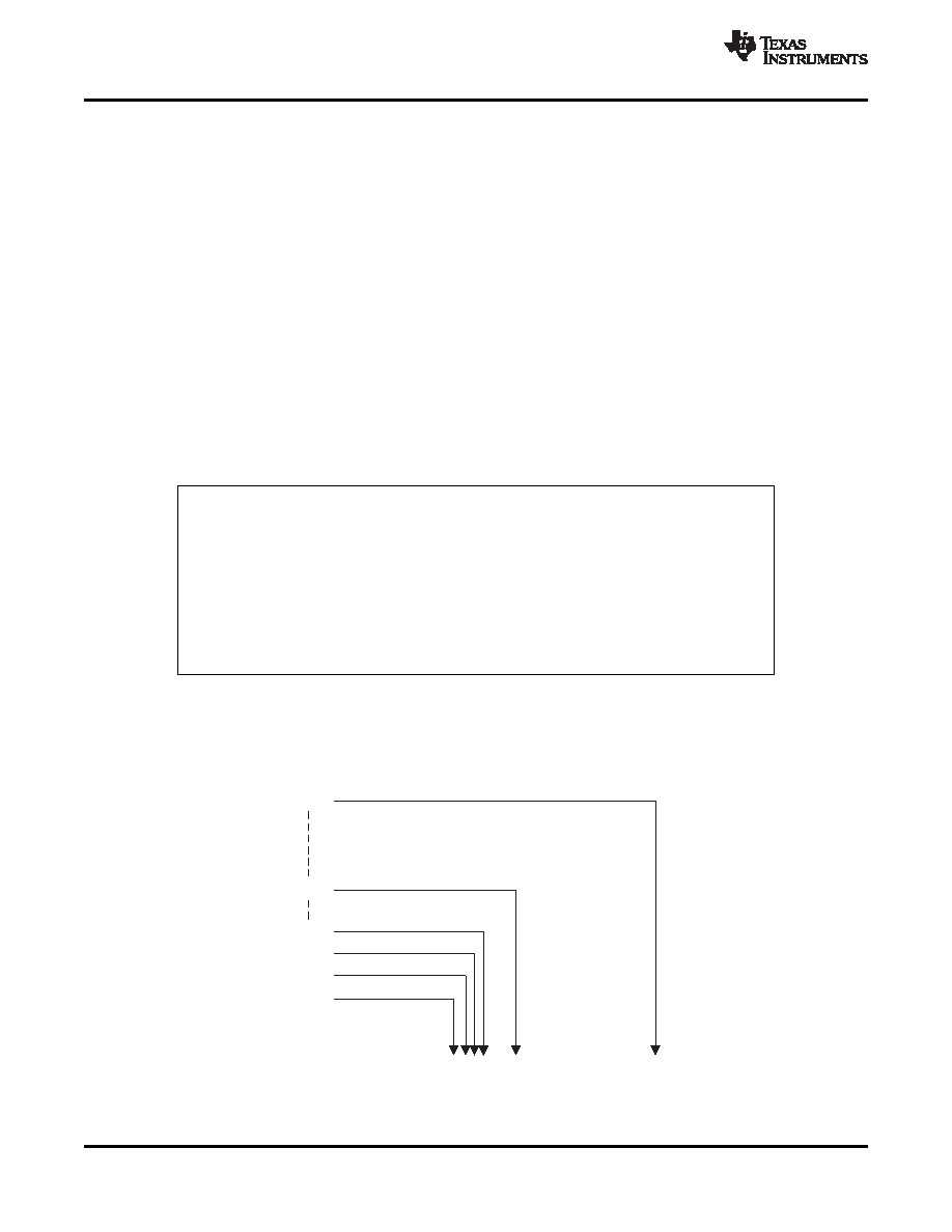
26-Bit 3.23 Number Format
2
Bit
–23
S_xx.xxxx_xxxx_xxxx_xxxx_xxxx_xxx
2
Bit
–5
2
Bit
–1
2 Bit
0
SignBit
2 Bit
1
M0125-01
SLOS605 – JANUARY 2009............................................................................................................................................................................................... www.ti.com
The TAS5710 uses an approach called bank switching together with automatic sample-rate detection. All
processing features that must be changed for different sample rates are stored internally in the TAS5710. The
TAS5710 has three full banks storing information, one for 32-48 kHz, one for 16-24 kHz, and one for all other
data rates. Combined with the clock-rate autodetection feature, bank switching allows the TAS5710 to detect
automatically a change in the input sample rate and switch to the appropriate bank without any MCU
intervention.
An external controller updates the three banks (see the I2C register mapping table for bankable locations) during
the initialization sequence.
If the autobank switch is enabled (register 0x50, bits 2:0) , then the TAS5710 automatically swaps the
coefficients for subsequent sample rate changes, avoiding the need for any external controller intervention for a
sample rate change.
By default, bits 2:0 have the value 000; that means the bank switch is disabled. In that state, any update to
locations 0x29–0x3F and 0x58–0x5F go into the DAP. A write to register 0x50 with bits 2:0 being 001, 010, or
011 brings the system into the coefficient-bank-update state update bank1, update bank2, or update bank3,
respectively. Any subsequent write to locations 0x29-0x3F and 0x58–0x5F updates the coefficient banks stored
outside the DAP. After updating all the three banks, the system controller should issue a write to register 0x50
with bits 2:0 being 100; this changes the system state to automatic bank update. In automatic bank update, the
TAS5710 automatically swaps banks based on the sample rate.
Command sequences for initialization can be summarized as follows:
1.
Enable factory trim for internal oscillator: Write to register 0x1B with a value 0x00.
2.
Update coefficients: Coefficients can be loaded into DAP RAM using the manual bank mode.
OR
Use automatic bank mode.
a.
Enable bank-1 mode: Write to register 0x50 with 0x01. Load the 32 kHz coefficients.
b.
Enable bank-2 mode: Write to register 0x50 with 0x02. Load the 48 kHz coefficients.
c.
Enable bank-3 mode: Write to register 0x50 with 0x03. Load the other coefficients.
d.
Enable automatic bank switching by writing to register 0x50 with 0x04.
3.
Bring the system out of all-channel shutdown: Write 0 to bit 6 of register 0x05.
4.
Issue master volume: Write to register 0x07 with the volume value (0 db = 0x30).
All mixer gain coefficients are 26-bit coefficients using a 3.23 number format. Numbers formatted as 3.23
numbers means that there are 3 bits to the left of the decimal point and 23 bits to the right of the decimal point.
This is shown in Figure 35 .
Figure 35. 3.23 Format
28
Copyright 2009, Texas Instruments Incorporated
Product Folder Link(s): TAS5710
相關PDF資料 |
PDF描述 |
|---|---|
| TAS5715PHPR | 41.5 W, 2 CHANNEL, AUDIO AMPLIFIER, PQFP48 |
| TAS5715PHP | 41.5 W, 2 CHANNEL, AUDIO AMPLIFIER, PQFP48 |
| TAS5716PAPR | 20.6 W, 2 CHANNEL, AUDIO AMPLIFIER, PQFP64 |
| TAS5716PAP | 20.6 W, 2 CHANNEL, AUDIO AMPLIFIER, PQFP64 |
| TAS5719PHPR | 15 W, 2 CHANNEL, AUDIO AMPLIFIER, PQFP48 |
相關代理商/技術參數(shù) |
參數(shù)描述 |
|---|---|
| TAS5710PHP | 制造商:Texas Instruments 功能描述:Audio Power Amplifier IC 制造商:Texas Instruments 功能描述:IC, AUDIO PWR AMP, CLASS D, 20W HTQFP-48 |
| TAS5710PHPR | 功能描述:音頻放大器 20W St Closed-loop I2S Audio Amp RoHS:否 制造商:STMicroelectronics 產(chǎn)品:General Purpose Audio Amplifiers 輸出類型:Digital 輸出功率: THD + 噪聲: 工作電源電壓:3.3 V 電源電流: 最大功率耗散: 最大工作溫度: 安裝風格:SMD/SMT 封裝 / 箱體:TQFP-64 封裝:Reel |
| TAS5711 | 制造商:TI 制造商全稱:Texas Instruments 功能描述:20-W DIGITAL AUDIO-POWER AMPLIFIER WITH EQ, DRC, AND 2.1 MODE |
| TAS5711PHP | 功能描述:音頻放大器 2-Channel Dig Audio Amp RoHS:否 制造商:STMicroelectronics 產(chǎn)品:General Purpose Audio Amplifiers 輸出類型:Digital 輸出功率: THD + 噪聲: 工作電源電壓:3.3 V 電源電流: 最大功率耗散: 最大工作溫度: 安裝風格:SMD/SMT 封裝 / 箱體:TQFP-64 封裝:Reel |
| TAS5711PHP | 制造商:Texas Instruments 功能描述:Audio Power Amplifier IC 制造商:Texas Instruments 功能描述:IC, AUDIO PWR AMP, CLASS D, 20W HTQFP-48 |
發(fā)布緊急采購,3分鐘左右您將得到回復。