- 您現(xiàn)在的位置:買賣IC網(wǎng) > PDF目錄98162 > TAS5182IDCAR (TEXAS INSTRUMENTS INC) 100 W, 2 CHANNEL, AUDIO AMPLIFIER, PDSO56 PDF資料下載
參數(shù)資料
| 型號(hào): | TAS5182IDCAR |
| 廠商: | TEXAS INSTRUMENTS INC |
| 元件分類: | 音頻/視頻放大 |
| 英文描述: | 100 W, 2 CHANNEL, AUDIO AMPLIFIER, PDSO56 |
| 封裝: | GREEN, PLASTIC, HTSSOP-56 |
| 文件頁數(shù): | 2/21頁 |
| 文件大小: | 705K |
| 代理商: | TAS5182IDCAR |

TAS5182
SLES045E - JUNE 2002 - REVISED MAY 2004
www.ti.com
10
TAS5182 Power Up and Reset
After power up, all gate drive outputs are held low (i.e., the
error latch is set). Normal operation can be initiated by
toggling RESET_AB and/or RESET_CD from a low state
to a high state. If no errors are present, then the TAS5182
device is ready to accept audio inputs.
TAS5182 Reset and Error Timing
The TAS5182 device provides two output control
configurations for reset and error situations. In a BTL
system configuration, the MOSFET outputs must be
grounded before resuming normal operation. This enables
the bootstrap capacitors to charge.
Reset and Error Timing (BTL System)
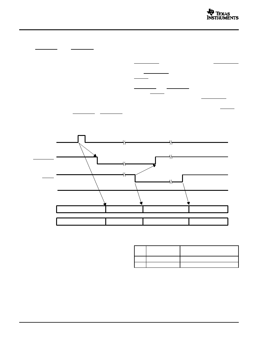
When using this device in the BTL configuration, it is
advisable to bring the MOSFET outputs to a high
impedance state when reset (RESET_AB or RESET_CD)
is asserted. Figure 4 shows the timing that occurs in this
configuration. This feature is enabled by connecting the
LOW/HIZ terminal to DVSS.
When an error event occurs (see Table 1) and following
propagation delay tpd(E-SD), the TAS5182 device pulls the
SHUTDOWN signal low. The falling edge of SHUTDOWN
forces the MOSFET outputs into a high-impedance state.
The SHUTDOWN signal is usually connected to the
RESET terminal of the TAS50XX PWM controller. After
some delay, the controller then asserts the TAS5182
RESET_AB and RESET_CD terminals low. The falling
edge of RESET forces the MOSFET outputs to ground
potential (this event also brings the SHUTDOWN signal
high). This allows the bootstrap capacitors to charge
through the grounded MOSFET outputs. When RESET is
pulled high, the system resumes normal operation.
TAS5182
Outputs
Error Event
LOW/HIZ = LOW
MOSFET
Outputs
HI-Z
SHUTDOWN
RESET
Normal Operation
All Gate Outputs Low
Normal Operation
tpd(E-SD)
tpd(E-L)
tpd(R-LH)
tpd(R-SD)
tpd(R-OP)
Figure 4. Reset and Error Timing (BTL System)
Overcurrent Configuration From Circuit
The output current flows through internal resistance
RDS(on) of the external MOSFETs, which creates voltage
drop VDS. The overcurrent detector senses this voltage to
trigger an error event. The exact current limit depends on
parasitics from the PCB layout, resistance of the MOSFET
at the operation temperature, and the configuration of the
H-bridge output stage.
See Table 2 for the OCL and OCH reference voltages.
Figure 5
shows
the
recommended
overcurrent
configuration circuit.
Table 2. OCL and OCH Reference Voltages
(Overcurrent Configuration Circuit)
VOLTAGE
OUTPUT INDUCTOR SHUTDOWN
CURRENT RANGE(1)
OCL
0.7 V (terminal 27)
12-19 A
OCH
1.17 V (terminal 8)
14-24 A
(1) Measured on Texas Instruments reference board
TAS5182C6REF.
相關(guān)PDF資料 |
PDF描述 |
|---|---|
| TAS5182DCARG4 | 100 W, 2 CHANNEL, AUDIO AMPLIFIER, PDSO56 |
| TAS5182IDCAG4 | 100 W, 2 CHANNEL, AUDIO AMPLIFIER, PDSO56 |
| TAS5182IDCARG4 | 100 W, 2 CHANNEL, AUDIO AMPLIFIER, PDSO56 |
| TAS5186ADDVR | 60 W, 6 CHANNEL, AUDIO AMPLIFIER, PDSO44 |
| TAS5186ADDV | 60 W, 6 CHANNEL, AUDIO AMPLIFIER, PDSO44 |
相關(guān)代理商/技術(shù)參數(shù) |
參數(shù)描述 |
|---|---|
| TAS5182IDCARG4 | 功能描述:音頻放大器 Dig Amp Pwr Stage Controller RoHS:否 制造商:STMicroelectronics 產(chǎn)品:General Purpose Audio Amplifiers 輸出類型:Digital 輸出功率: THD + 噪聲: 工作電源電壓:3.3 V 電源電流: 最大功率耗散: 最大工作溫度: 安裝風(fēng)格:SMD/SMT 封裝 / 箱體:TQFP-64 封裝:Reel |
| TAS5186 | 制造商:TI 制造商全稱:Texas Instruments 功能描述:6-Channel, 210-W, Digital-Amplifier Power Stage |
| TAS5186A | 制造商:TI 制造商全稱:Texas Instruments 功能描述:6-Channel, 210-W, Digital-Amplifier Power Stage |
| TAS5186ADDV | 功能描述:音頻放大器 6-Ch 210-W Digital PowerStage RoHS:否 制造商:STMicroelectronics 產(chǎn)品:General Purpose Audio Amplifiers 輸出類型:Digital 輸出功率: THD + 噪聲: 工作電源電壓:3.3 V 電源電流: 最大功率耗散: 最大工作溫度: 安裝風(fēng)格:SMD/SMT 封裝 / 箱體:TQFP-64 封裝:Reel |
| TAS5186ADDV | 制造商:Texas Instruments 功能描述:Audio Power Amplifier IC |
發(fā)布緊急采購,3分鐘左右您將得到回復(fù)。