- 您現(xiàn)在的位置:買賣IC網(wǎng) > PDF目錄383878 > TAS5100ADAPR (Texas Instruments, Inc.) Single Audio Amplifier PDF資料下載
參數(shù)資料
| 型號: | TAS5100ADAPR |
| 廠商: | Texas Instruments, Inc. |
| 元件分類: | 運(yùn)動控制電子 |
| 英文描述: | Single Audio Amplifier |
| 中文描述: | 單音頻放大器 |
| 文件頁數(shù): | 11/16頁 |
| 文件大小: | 214K |
| 代理商: | TAS5100ADAPR |
TAS5100A
SLES030
–
FEBRUARY 2002
11
www.ti.com
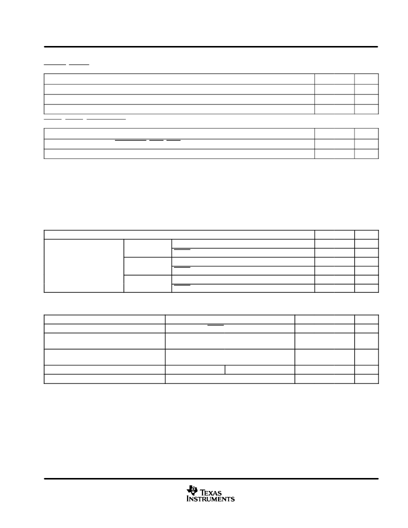
static digital specifications
RESET, PWDN, PWM_AP, PWM_AM, PWM_BP, PWM_BM, T
A
= 25
°
C, DVDD = 3.3 V
PARAMETERS
MIN
MAX
UNIT
High-level input voltage, VIH
Low-level input voltage, VIL
Input leakage current
2
V
0.8
V
–
10
10
μ
A
ERR0, ERR1, SHUTDOWN, (open drain with internal pullup resistor) T
A
= 25
°
C, DVDD = 3.3 V)
PARAMETERS
MIN
MAX
UNIT
Internal pullup resistors from SHUTDOWN, ERR0, ERR1 to DVDD
15
k
Low-level output voltage (IO = 4 mA), VOL
0.4
V
TAS5000/TAS5100A system performance measured at the speaker terminals
See the TI Literature Number SLAA117 for TAS5000/TAS5100A system performance.
electrical characteristics
supply, T
A
= 25
°
C (F
switching
= 384 kHz, OUTPUTA and OUTPUTB not connected, DVDD = 3.3 V,
PVDDA1 = 25 V, PVDDB1 = 25 V, PVDDA2 = 22 V, PVDDB2 = 22 V, 50% input duty cycle)
PARAMETER
Operating
TYP
MAX
UNIT
mA
μ
A
mA
μ
A
mA
μ
A
DVDD
2
PWDN = 0
Operating
500
Supply current
PVDDA1
PVDDB1
6.3
PWDN = 0
25
PVDDA2
PVDDB2
Operating
PWDN = 0
6.5
250
13-k
resistor from BIAS_A (pin 11) to DVSS and 13-k
resistor from BIAS_B (pin 12) to DVSS.
H-Bridge transistors, PVDDA2 = PVDDB2 = 22 V, DVDD = 3.3 V, T
A
= 25
°
C (unless otherwise noted)
PARAMETER
TEST CONDITIONS
MIN
TYP
MAX
UNIT
Drain-to-source breakdown voltage
ID = 1 mA, PWDN = 0, Hi-Z state
ISINK = 2.5 A,
See Notes 2, 3, and 4,
28
V
Forward on-state resistance, low side drivers
OUTPUTA and OUTPUTB to PVSS
PWM_AP = PWM_BP = 0,
PWM_AM = PWM_BM = 1
0.2
Forward on-state resistance, high side drivers
PVDDA1 to OUTPUTA, PVDDB1 to OUTPUTB
ISOURCE = 2.5 A,
See Notes 2, 3, and 5,
PWM_AP = PWM_BP = 1,
PWM_AM = PWM_BM = 0
0.2
On-state resistance matching low-side drivers
98%
On-state resistance matching high-side drivers
98%
NOTES:
1. Test time should be < 1 ms to avoid temperature change.
2. These parameters are measured with voltage-sensing contacts separate from the current-carrying contacts.
3. Connect PVDDA2 and PVDDB2 to 22-V power supply with respect to PVSS. LDROUTA, LDROUTB, BOOTSTRAPA, and
BOOTSTRAPB pins open.
4. Connect PVDDA2 to 22-V power supply with respect to PVSS. LDROUTA, LDROUTB, BOOTSTRAPA and BOOTSTRAPB
capacitors are connected respectively. Clock PWM inputs to allow bootstrap capacitors to charge. 93
–
99% modulation must be used
on PWM_AP, PWM_AM, PWM_BP, and PWM_BM inputs to prevent the activity detector from shutting down the device during this
measurement. Note that Fswitching = 384 kHz.
相關(guān)PDF資料 |
PDF描述 |
|---|---|
| TAS5100AIDAP | Single Audio Amplifier |
| TAS5110ADADR | PurePath Digital AMPLIFIER TAS5110A 50-W DIGITAL AMPLIFIER POWER STAGE |
| TB28F004S3-150 | BYTE-WIDE SMART 3 FlashFile MEMORY FAMILY 4, 8, AND 16 MBIT |
| TB28F008S3-150 | BYTE-WIDE SMART 3 FlashFile MEMORY FAMILY 4, 8, AND 16 MBIT |
| TB28F004S5-100 | BYTE-WIDE SMART 5 FlashFile MEMORY FAMILY 4, 8, AND 16 MBIT |
相關(guān)代理商/技術(shù)參數(shù) |
參數(shù)描述 |
|---|---|
| TAS5100ADAPRG4 | 制造商:TI 制造商全稱:Texas Instruments 功能描述:TRUE DIGITAL AUDIO AMPLIFIER TAS5100A PWM POWER OUTPUT STAGE |
| TAS5100AIDAP | 制造商:Rochester Electronics LLC 功能描述:TAS5100AI - Bulk 制造商:Texas Instruments 功能描述: |
| TAS5100AIDAPR | 制造商:TI 制造商全稱:Texas Instruments 功能描述:TRUE DIGITAL AUDIO AMPLIFIER TAS5100A PWM POWER OUTPUT STAGE |
| TAS5100AIDAPRG4 | 制造商:TI 制造商全稱:Texas Instruments 功能描述:TRUE DIGITAL AUDIO AMPLIFIER TAS5100A PWM POWER OUTPUT STAGE |
| TAS5100DAP | 制造商:Rochester Electronics LLC 功能描述:- Bulk 制造商:Texas Instruments 功能描述: |
發(fā)布緊急采購,3分鐘左右您將得到回復(fù)。