- 您現(xiàn)在的位置:買賣IC網(wǎng) > PDF目錄385896 > TA1316AN (Toshiba Corporation) YCbCr/YPbPr Signal and Sync Processor for Digital TV, Progressive Scan TV and Double Scan TV PDF資料下載
參數(shù)資料
| 型號(hào): | TA1316AN |
| 廠商: | Toshiba Corporation |
| 英文描述: | YCbCr/YPbPr Signal and Sync Processor for Digital TV, Progressive Scan TV and Double Scan TV |
| 中文描述: | YCbCr /色差信號(hào)處理器和同步數(shù)字電視,逐行掃描電視和雙掃描電視 |
| 文件頁數(shù): | 97/115頁 |
| 文件大小: | 1399K |
| 代理商: | TA1316AN |
第1頁第2頁第3頁第4頁第5頁第6頁第7頁第8頁第9頁第10頁第11頁第12頁第13頁第14頁第15頁第16頁第17頁第18頁第19頁第20頁第21頁第22頁第23頁第24頁第25頁第26頁第27頁第28頁第29頁第30頁第31頁第32頁第33頁第34頁第35頁第36頁第37頁第38頁第39頁第40頁第41頁第42頁第43頁第44頁第45頁第46頁第47頁第48頁第49頁第50頁第51頁第52頁第53頁第54頁第55頁第56頁第57頁第58頁第59頁第60頁第61頁第62頁第63頁第64頁第65頁第66頁第67頁第68頁第69頁第70頁第71頁第72頁第73頁第74頁第75頁第76頁第77頁第78頁第79頁第80頁第81頁第82頁第83頁第84頁第85頁第86頁第87頁第88頁第89頁第90頁第91頁第92頁第93頁第94頁第95頁第96頁當(dāng)前第97頁第98頁第99頁第100頁第101頁第102頁第103頁第104頁第105頁第106頁第107頁第108頁第109頁第110頁第111頁第112頁第113頁第114頁第115頁
TA1316AN
2002-10-04
97
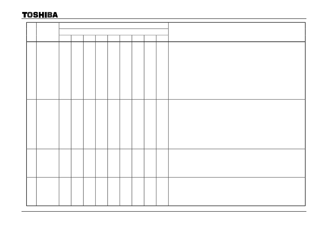
Test Conditions
SW mode
Note
No.
Parameter
SW3
SW4
SW5
SW33
SW34 SW35 SW37 SW38 SW39
Test Method (test conditions: V
CC
=
9 V/2 V, Ta
=
25°
±
3°C)
T26 Text ACL
characteristic
A
B
B
A
A
B
A
A
A
(1) Apply 5 V from external power supply to pin 49.
(2) Input signal 1 (f
0
=
100 kHz, picture period amplitude
=
0.2 V
P-P
) to pin 35.
(3) Measure pin 43 picture period amplitude vTXACL1.
(4) Apply external power supply (pin 53 DC voltage
0.5 V) to pin 53 and measure picture
period amplitude output vTXACL2 on pin 43.
(5) Apply external power supply (pin 53 DC voltage
1.0 V) to pin 53 and measure picture
period amplitude output vTXACL3 on pin 43.
(6) TXACL
1
=
20
×
og
TXACL
2
=
20
×
og
"
(vTXACL2/vTXACL1)
"
(vTXACL3/vTXACL1)
(7) Repeat steps (5) and (6), setting sub-address (10) data to 01 to ascertain TXACL
3
and
TXACL
4.
T27 Analog OSD
gain
A
B
B
A
A
A
A
or
B
A
or
B
A
or
B
(1) Input signal 1 (f
0
=
100 kHz, picture period amplitude
=
0.2 V
P-P
) to pin 3 and adjust DRIVE
GAIN 1/2 so that pin 41/42 picture period amplitude is equal to that of pin 43.
(2) Apply 5 V from external power supply to pins 50 and 51.
(3) Input signal 1 (f
0
=
100 kHz, picture period amplitude
=
0.2 V
P-P
) to pin 39.
(4) Adjust output picture period amplitude v43R on pin 43.
(5) Repeat steps (3) and (4), making the following changes:
Input to pin 38 and measure picture period amplitude output on pin 42 (v42G).
Input to pin 37 and measure picture period amplitude output on pin 41 (v41B).
(6) Calculate using the following formulae.
G
OSDR
=
v43R/0.2
G
OSDG
=
v42G/0.2
G
OSDB
=
v41B/0.2
T28 Analog OSD
white peak
slice level
A
B
B
A
A
A
A
A
A
(1) Apply 5 V from external power supply to pins 50 and 51.
(2) Apply external power supply to pin 39 and gradually increase voltage from 4.5 V DC. When
pin 43 output is clipped, measure picture period amplitude.
(3) Repeat step (2), making the following changes:
Input to pin 38 and measure picture period amplitude output on pin 42.
Input to pin 37 and measure picture period amplitude output on pin 41.
T29 Analog OSD
black peak
limit level
A
B
B
A
A
A
A
A
A
(1) Apply 5 V from external power supply to pins 50 and 51.
(2) Apply external power supply to pin 39 and gradually decrease voltage from 4.5 V DC. When
pin 43 output is clipped, measure picture period amplitude.
(3) Repeat step (2), making the following changes.
Input to pin 38 and measure picture period amplitude output on pin 42.
Input to pin 37 and measure picture period amplitude output on pin 41.
相關(guān)PDF資料 |
PDF描述 |
|---|---|
| TA15.0 | MU-MU FIBER JUMPER SINGLE MODE PVC 5 METER |
| TA10.0 | Beldsol Magnet Wire, Approx. Spool Length: 4060'; Conductor Size AWG:34; Approval Categories:J-W-1177/9; MW 28-C (Single); Conductor Material:Copper; Features:Dual-Insulated with Polyurethane and Nylon Overcoating; Solderable RoHS Compliant: Yes |
| TA2.0 | HIGH-ENERGY TRIGGERED SPARK GAPS |
| TA7.0 | HIGH-ENERGY TRIGGERED SPARK GAPS |
| TA5.0 | HIGH-ENERGY TRIGGERED SPARK GAPS |
相關(guān)代理商/技術(shù)參數(shù) |
參數(shù)描述 |
|---|---|
| TA1317AFG | 制造商:TOSHIBA 制造商全稱:Toshiba Semiconductor 功能描述:Deflection Processor IC for TV |
| TA1317AN | 制造商:TOSHIBA 制造商全稱:Toshiba Semiconductor 功能描述:Deflection Processor IC for TV |
| TA1317ANG | 制造商:TOSHIBA 制造商全稱:Toshiba Semiconductor 功能描述:Deflection Processor IC for TV |
| TA1318AF | 制造商:TOSHIBA 制造商全稱:Toshiba Semiconductor 功能描述:SYNC Processor, Frequency Counter IC for TV Component Signals |
| TA1318AFG | 制造商:TOSHIBA 制造商全稱:Toshiba Semiconductor 功能描述:SYNC Processor, Frequency Counter IC for TV Component Signals |
發(fā)布緊急采購,3分鐘左右您將得到回復(fù)。