- 您現(xiàn)在的位置:買賣IC網(wǎng) > PDF目錄361357 > T81L0003A-AD (TM Technology, Inc.) Reduced I/O 8-bit MCU PDF資料下載
參數(shù)資料
| 型號: | T81L0003A-AD |
| 廠商: | TM Technology, Inc. |
| 英文描述: | Reduced I/O 8-bit MCU |
| 中文描述: | 減少的I / O 8位微控制器 |
| 文件頁數(shù): | 8/20頁 |
| 文件大小: | 113K |
| 代理商: | T81L0003A-AD |
TE
CH
tm
Serial Data Buffer
T81L0003A
TM Technology, Inc. reserves the right
P. 8
to change products or specifications without notice. Revision: C
Publication Date: SEP. 2004
The Serial Buffer is actually two separate registers, a transmit buffer and a receive buffer. When data is moved to
SBUF, it goes to the transmit buffer and is held for serial transmission. (Moving a byte to SBUF is what initiates the
transmission.) When data is moved from SBUF, it comes from the receive buffer.
Timer Registers
Register pairs (TH0, TL0) is the 16-bit Counting registers for Timer/Counters 0, while (TH1, TL1) and (TH2, TL2)
are the 16-bit Counting registers for Timer1 and Timer2, respectively.
.
Control Register
Special Function Registers IP, IE, TMOD, TCON, SCON, and PCON contain control and status bits for the interrupt
system, the Timer/Counters, and the serial port. They are described in later sections.
Power Down Mode
The power down mode can be active by setting the PD bit (on PCON register) to 1 and the program status will keep
on the state before power down set. The MCU can be woken up by interrupt (I0 or I1) if the one is enable. After wake up,
need to clear PD bit to 0 on first instruction.
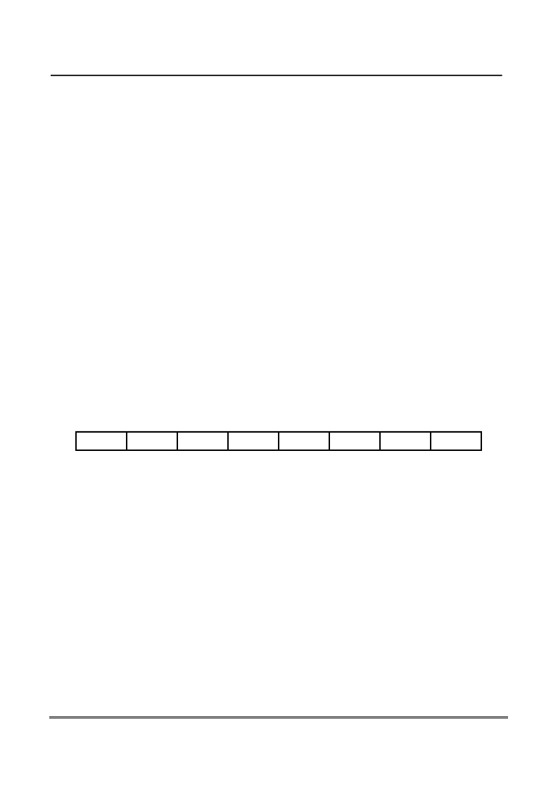
PCON (address: 87H)
MSB
LSB
SMOD
-
-
-
GF1
GF0
PD
-
Standard Serial Interface
The serial port is full duplex, meaning it can transmit and receive simultaneously. It is also receive-buffered, meaning
it can commence reception of a second byte before a previously received byte has been read from the register. (However, if
the first byte still hasn’t been read by the time reception of the second byte is complete, one of the bytes will be lost.) The
serial port receive and transmit registers are both accessed at Special Function Register SBUF. Writing to SBUF loads the
transmit register, and reading SBUF accesses a physically separate receive register.
The serial port can operate in 4 modes:
Mode 0:
Serial data enters and exits through RxD. TxD outputs the shift clock. 8 bits are transmitted/received (LSB first).
The baud rate is fixed at 1/12 the oscillator frequency.
Mode 1:
10 bits are transmitted (through TxD) or received (through RxD): a start bit (0), 8 data bits (LSB first), and a stop
bit (1). On receive, the stop bit goes into RB8 in Special Function Register SCON. The baud rate is variable.
Mode 2:
11 bits are transmitted (through TxD) or received (through RxD): start bit (0), 8 data bits (LSB first), a
programmable 9th data bit, and a stop bit (1). On Transmit, the 9th data bit (TB8 in SCON) can be assigned the value of 0
or 1. Or, for example, the parity bit (P, in the PSW) could be moved into TB8. On receive, the 9th data bit goes into RB8 in
相關(guān)PDF資料 |
PDF描述 |
|---|---|
| T81L0003B | 8-bit MCU |
| T81L0003B-AD | 8-bit MCU |
| T81L0003B-AK | 8-bit MCU |
| T81L0003B-BD | 8-bit MCU |
| T81L0003B-BK | 8-bit MCU |
相關(guān)代理商/技術(shù)參數(shù) |
參數(shù)描述 |
|---|---|
| T81L0003A-AK | 制造商:TMT 制造商全稱:TMT 功能描述:Reduced I/O 8-bit MCU |
| T81L0003A-BD | 制造商:TMT 制造商全稱:TMT 功能描述:Reduced I/O 8-bit MCU |
| T81L0003A-BK | 制造商:TMT 制造商全稱:TMT 功能描述:Reduced I/O 8-bit MCU |
| T81L0003B | 制造商:TMT 制造商全稱:TMT 功能描述:8-bit MCU |
| T81L0003B-AD | 制造商:TMT 制造商全稱:TMT 功能描述:8-bit MCU |
發(fā)布緊急采購,3分鐘左右您將得到回復。