- 您現(xiàn)在的位置:買賣IC網(wǎng) > PDF目錄385882 > SY100E310JI (Micrel Semiconductor,Inc.) 3.3V ECL/PECL 2:8 DIFFERENTIAL FANOUT BUFFER PDF資料下載
參數(shù)資料
| 型號: | SY100E310JI |
| 廠商: | Micrel Semiconductor,Inc. |
| 英文描述: | 3.3V ECL/PECL 2:8 DIFFERENTIAL FANOUT BUFFER |
| 中文描述: | 3.3 ECL / PECL的2:8扇出緩沖器差 |
| 文件頁數(shù): | 4/6頁 |
| 文件大小: | 78K |
| 代理商: | SY100E310JI |
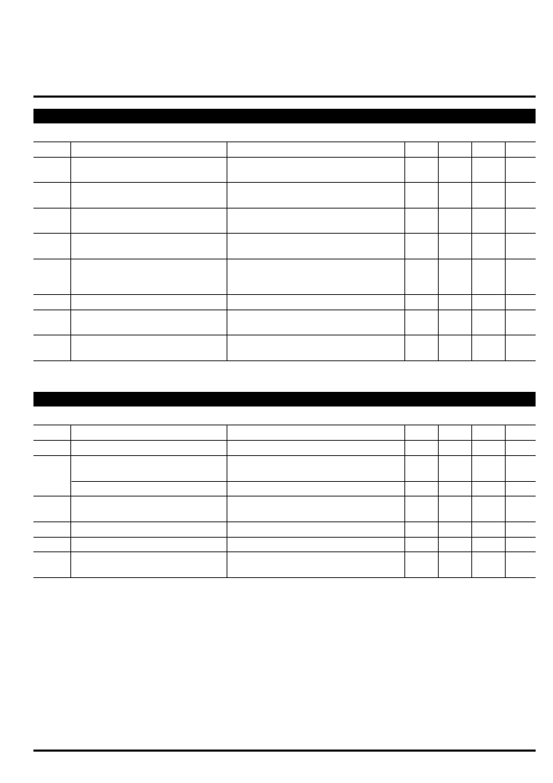
4
SY100E310L
Micrel, Inc.
M9999-032206
hbwhelp@micrel.com or (408) 955-1690
V
CC
= +3.3V, V
EE
= 0V; T
A
=
–
40
°
C to +85
°
C; unless noted.
Symbol
Parameter
Condition
Min
Typ
Max
Units
V
OH
Output High Voltage
(Q0-Q7, /Q0-/Q7)
R
L
= 50
to V
CC
–
2V
–
1085
–
955
–
880
mV
V
OL
Output Low Voltage
(Q0-Q7, /Q0-/Q7)
R
L
= 50
to V
CC
–
2V
–
1830
–
1705
–
1620
mV
V
IH
Input High Voltage
(CLKA, /CLKA, CLKB, /CLKB, CLK_SEL)
–
1165
–
880
mV
V
IL
Input Low Voltage
(CLKA, /CLKA, CLKB, /CLKB, CLK_SEL)
–
1810
–
1475
mV
V
IHCMR
Input High Voltage Common
Mode Range (Differential)
(CLKA, / CLKA, CLKB, /CLKB)
Note 9
–
1.5
–
0.4
V
V
BB
I
IN
Output Reference Voltage
–
1.38
–
1.26
V
Input HIGH Current
(CLKA, /CLKA, CLKB,/CLKB, CLK_SEL)
150
μ
A
I
IL
Input LOW Current
(CLKA, /CLKA, CLKB, /CLKB, CLK_SEL)
0.5
μ
A
LVNECL DC ELECTRICAL CHARACTERISTICS
(7, 8)
V
CC
= +3.0 to +3.6V and V
EE
= 0V or V
CC
= 0V and V
EE
=
–
3.0 to
–
3.6V; T
A
=
–
40
°
C to +85
°
C; unless noted.
Symbol
Parameter
Condition
Min
Typ
Max
Units
f
MAX
t
PD
Maximum Operating Frequency
V
OUT
= 400mV
Note 10
800
MHz
Propagation Delay
CLKA-to-Q, CLKB-to-Q (Differential)
525
725
ps
CLKA-to-Q, CLKB-to-Q (Single-ended)
Note 11
500
750
ps
t
SKEW
Within-Device Skew
Part-to-Part Skew (Differential)
Note 12
50
200
ps
ps
t
JITTER
V
PP
t
r
, t
f
Cycle-to-Cycle Jitter
1
ps
RMS
mV
Input Swing
Note 13
500
1000
Rise / Fall Time (20% to 80%)
(Q0-Q7, /Q0-/Q7)
160
375
600
ps
Notes:
7. The circuit is designed to meet the DC specifications shown in the above table after thermal equilibrium has been established.
8. Input and output parameters vary 1:1 with V
CC
. V
CC
can vary
±
0.3V.
9. V
is defined as the range within which the V
level may vary with the device still meeting the propagation delay specification. The V
IL
level
must be such that the peak-to-peak voltage is less than 1.0V and then greater than or equal to V
PP
(min).
10. The differential propagation delay is defined as the delay from the crossing points of the differential input signals to the crossing point of the
differential output signals.
11. The single-ended propagation delay is defined as the delay from the 50% point of the input signal to the 50% point of the output signal.
12. The within-device skew is defined as the worst case difference between any two similar delay paths within a single device.
13. V
(min) is defined as the minimum input differential voltage which will cause no increase in the propagation delay. The V
PP
(min) is AC limited for
the E310L as a differential input as low as 50 mV will still produce full ECL levels at the output.
AC ELECTRICAL CHARACTERISTICS
相關(guān)PDF資料 |
PDF描述 |
|---|---|
| SY100E310JITR | 3.3V ECL/PECL 2:8 DIFFERENTIAL FANOUT BUFFER |
| SY100E310JY | 3.3V ECL/PECL 2:8 DIFFERENTIAL FANOUT BUFFER |
| SY100E310JYTR | 3.3V ECL/PECL 2:8 DIFFERENTIAL FANOUT BUFFER |
| SY100E310LJI | 3.3V ECL/PECL 2:8 DIFFERENTIAL FANOUT BUFFER |
| SY100E310LJITR | 3.3V ECL/PECL 2:8 DIFFERENTIAL FANOUT BUFFER |
相關(guān)代理商/技術(shù)參數(shù) |
參數(shù)描述 |
|---|---|
| SY100E310JITR | 制造商:MICREL 制造商全稱:Micrel Semiconductor 功能描述:3.3V ECL/PECL 2:8 DIFFERENTIAL FANOUT BUFFER |
| SY100E310JY | 制造商:MICREL 制造商全稱:Micrel Semiconductor 功能描述:3.3V ECL/PECL 2:8 DIFFERENTIAL FANOUT BUFFER |
| SY100E310JYTR | 制造商:MICREL 制造商全稱:Micrel Semiconductor 功能描述:3.3V ECL/PECL 2:8 DIFFERENTIAL FANOUT BUFFER |
| SY100E310L | 制造商:MICREL 制造商全稱:Micrel Semiconductor 功能描述:3.3V ECL/PECL 2:8 DIFFERENTIAL FANOUT BUFFER |
| SY100E310L_0607 | 制造商:MICREL 制造商全稱:Micrel Semiconductor 功能描述:3.3V ECL/PECL 2:8 DIFFERENTIAL FANOUT BUFFER |
發(fā)布緊急采購,3分鐘左右您將得到回復(fù)。