- 您現(xiàn)在的位置:買(mǎi)賣(mài)IC網(wǎng) > PDF目錄372385 > SW-277RTR High Power GaAs SPDT Switch DC - 2.5 GHz PDF資料下載
參數(shù)資料
| 型號(hào): | SW-277RTR |
| 英文描述: | High Power GaAs SPDT Switch DC - 2.5 GHz |
| 中文描述: | 高功率GaAs SPDT開(kāi)關(guān)直流- 2.5吉赫 |
| 文件頁(yè)數(shù): | 1/2頁(yè) |
| 文件大小: | 29K |
| 代理商: | SW-277RTR |
High Power GaAs SPDT Switch
DC - 2.5 GHz
SW-277
V3.00
M/A-COM, Inc.
North America:
Tel. (800) 366-2266
Fax (800) 618-8883
I
Asia/Pacific: Tel. +81 3 3263 8761
Fax +81 3 3263 8769
I
Europe: Tel. +44 (1344) 869 595
Fax +44 (1344) 300 020
1
Specifications Subject to Change Without Notice.
Features
Positive Supply and Control Voltages
+36 dBm Typ. 1 dB Compression Point, 8V Supply
+65 dBm Typ. 3rd Order Intercept Point, 8V Supply
Low Insertion Loss: 0.4 dB Typical
Low Power Consumption: 100 μW
Fast Switching Speed
Tape and Reel Packaging Available
1
Description
M/A-COM’s SW-277 is a GaAs MMIC SPDT switch in a low cost
SOIC 8-lead surface mount plastic package. The SW-277 is ideally
suited for use where very low power consumption is required.
Typical applications include transmit/receive switching,
switch matrices, and filter banks in systems such as: radio and
cellular equipment, PCM, GPS, fiber optic modules, and other
battery powered radio equipment.
The SW-277 is fabricated with a monolithic GaAs MMIC using a
mature 1-micron process. The process features full chip
passivation for increased performance and reliability.
Electrical Specifications,
T
A
= +25°C
0°-8°
.0075-0.0098
(0.19-0.25)
.1890-.1968
(4.80-5.00)
- A -
.0099-0.0196
x 45° Chamfer
(0.25-0.50)
.2284-.2440
(5.80-6.20)
.010(0.25) M B M
PIN 8
Orientation
mark
PIN 1
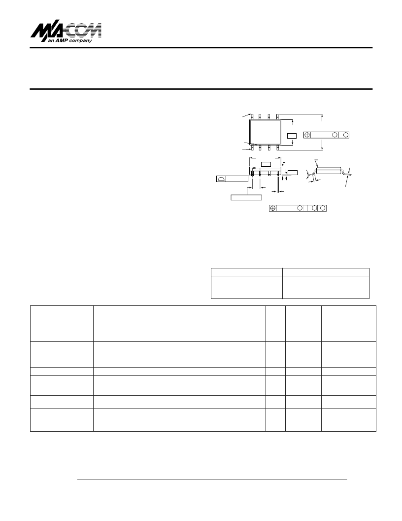
8- Lead SOP outline dimensions
Narrow body .150
(All dimensions per JEDEC No. MS-012-AA, Issue C)
Dimensions in ( ) are in mm.
Unless Otherwise Noted: .xxx = ± 0.010 (.xx = ± 0.25)
.xx = ± 0.02 (.x = ±0.5)
.1497-.1574
(3.80-4.00)
- B -
.050(1.27) BSC.
.013-.020 TYP.
(0.33-0.51)
.0040-.0098
(0.10-0.25)
- C -
.0532-.0688
(1.35-1.75)
.016-.050
(0.40-1.27)
.010(0.25) M C A M B S
.004 (0.10)
SO-8
1.Refer to “Tape and Reel Packaging” Section, or contact factory.
2.All specifications apply when operated with bias voltages of 0V for Vin Low and 5 to 10V for Vin Hi, and 50 Ohm impedance at all RF ports,
unless otherwise specified. High power (greater than 1W) handling specifications apply to cold switches only. For input powers under 1W, hot
switching can be used. The high control voltage must be within +/- 0.2V of the supply voltage. The RF ports must be blocked outside of the pack-
age from ground or any other voltage.
Parameter
Test Conditions
2
Unit
Min.
Typ.
Max
Insertion Loss
DC – 2.0 GHz
DC – 1.0 GHz
DC – 0.5 GHz
DC – 0.1 GHz
DC – 2.0 GHz
DC – 1.0 GHz
DC – 0.5 GHz
DC – 0.1 GHz
DC – 2.0 GHz
dB
dB
dB
dB
dB
dB
dB
dB
0.6
0.4
0.35
0.2
16
32
38
38
1.2:1
30
35
12
33
35.8
61
65
0.8
0.6
0.5
0.4
Isolation
14
28
35
35
VSWR
Trise, Tfall
Ton, Toff
Transients
One dB
Compression Point
3rd Order
Intercept
10% to 90% RF, 90% to 10% RF
50% Control to 90% RF, 50% Control to 10% RF
In Band
Input Power (5V Supply/Control)
Input Power (8V Supply/Control)
Measured Relative (5V Supply/Control)
to Input Power (8V Supply/Control)
(for two-tone input power up to +10 dBm)
nS
nS
mV
dBm
dBm
dBm
dBm
0.9 GHz
0.9 GHz
0.9 GHz
0.9 GHz
Model Number
SW-277 PIN
SW-277TR
SW-277RTR
Package
SOIC 8-Lead Plastic Package
Forward Tape and Reel
Reverse Tape and Reel
Ordering Information
相關(guān)PDF資料 |
PDF描述 |
|---|---|
| SW-277 | THERMAL UNIT |
| SW-277PIN | THERMAL UNIT |
| SW-277TR | THERMAL UNIT |
| SW-279RTR | High Power GaAs SPDT Switch DC - 2.5 GHz |
| SW-279 | High Power GaAs SPDT Switch DC - 2.5 GHz |
相關(guān)代理商/技術(shù)參數(shù) |
參數(shù)描述 |
|---|---|
| SW-277TR | 制造商:MA-COM 制造商全稱:M/A-COM Technology Solutions, Inc. 功能描述:High Power GaAs SPDT Switch DC - 2.0 GHz |
| SW277VSHQ7-N12 | 制造商:Samson Technologies 功能描述:Concert 277 UHF Wireless True Diversity Dual Handheld Microphone |
| SW-279 | 制造商:MA-COM 制造商全稱:M/A-COM Technology Solutions, Inc. 功能描述:Drivers for GaAs FET Switches and Digital Attenuators |
| SW-279PIN | 制造商:MA-COM 制造商全稱:M/A-COM Technology Solutions, Inc. 功能描述:High Power GaAs SPDT Switch DC - 2.5 GHz |
| SW279RTR | 制造商:未知廠家 制造商全稱:未知廠家 功能描述:Interface IC |
發(fā)布緊急采購(gòu),3分鐘左右您將得到回復(fù)。