- 您現(xiàn)在的位置:買賣IC網(wǎng) > PDF目錄195889 > ST72C124J4B6 IC-ST7 MICROCONTROLLER PDF資料下載
參數(shù)資料
| 型號: | ST72C124J4B6 |
| 英文描述: | IC-ST7 MICROCONTROLLER |
| 中文描述: | 集成電路ST7微控制器 |
| 文件頁數(shù): | 63/153頁 |
| 文件大小: | 1988K |
| 代理商: | ST72C124J4B6 |
第1頁第2頁第3頁第4頁第5頁第6頁第7頁第8頁第9頁第10頁第11頁第12頁第13頁第14頁第15頁第16頁第17頁第18頁第19頁第20頁第21頁第22頁第23頁第24頁第25頁第26頁第27頁第28頁第29頁第30頁第31頁第32頁第33頁第34頁第35頁第36頁第37頁第38頁第39頁第40頁第41頁第42頁第43頁第44頁第45頁第46頁第47頁第48頁第49頁第50頁第51頁第52頁第53頁第54頁第55頁第56頁第57頁第58頁第59頁第60頁第61頁第62頁當(dāng)前第63頁第64頁第65頁第66頁第67頁第68頁第69頁第70頁第71頁第72頁第73頁第74頁第75頁第76頁第77頁第78頁第79頁第80頁第81頁第82頁第83頁第84頁第85頁第86頁第87頁第88頁第89頁第90頁第91頁第92頁第93頁第94頁第95頁第96頁第97頁第98頁第99頁第100頁第101頁第102頁第103頁第104頁第105頁第106頁第107頁第108頁第109頁第110頁第111頁第112頁第113頁第114頁第115頁第116頁第117頁第118頁第119頁第120頁第121頁第122頁第123頁第124頁第125頁第126頁第127頁第128頁第129頁第130頁第131頁第132頁第133頁第134頁第135頁第136頁第137頁第138頁第139頁第140頁第141頁第142頁第143頁第144頁第145頁第146頁第147頁第148頁第149頁第150頁第151頁第152頁第153頁
ST72334J/N, ST72314J/N, ST72124J
17/153
5 FLASH PROGRAM MEMORY
5.1 INTRODUCTION
FLASH devices have a single voltage non-volatile
FLASH memory that may be programmed in-situ
(or plugged in a programming tool) on a byte-by-
byte basis.
5.2 MAIN FEATURES
s
Remote In-Situ Programming (ISP) mode
s
Up to 16 bytes programmed in the same cycle
s
MTP memory (Multiple Time Programmable)
s
Read-out memory protection against piracy
5.3 STRUCTURAL ORGANISATION
The FLASH program memory is organised in a
single 8-bit wide memory block which can be used
for storing both code and data constants.
The FLASH program memory is mapped in the up-
per part of the ST7 addressing space and includes
the reset and interrupt user vector area .
5.4 IN-SITU PROGRAMMING (ISP) MODE
The FLASH program memory can be programmed
using Remote ISP mode. This ISP mode allows
the contents of the ST7 program memory to be up-
dated using a standard ST7 programming tools af-
ter the device is mounted on the application board.
This feature can be implemented with a minimum
number of added components and board area im-
pact.
An example Remote ISP hardware interface to the
standard ST7 programming tool is described be-
low. For more details on ISP programming, refer to
the ST7 Programming Specification.
Remote ISP Overview
The Remote ISP mode is initiated by a specific se-
quence on the dedicated ISPSEL pin.
The Remote ISP is performed in three steps:
– Selection of the RAM execution mode
– Download of Remote ISP code in RAM
– Execution of Remote ISP code in RAM to pro-
gram the user program into the FLASH
Remote ISP hardware configuration
In Remote ISP mode, the ST7 has to be supplied
with power (VDD and VSS) and a clock signal (os-
cillator and application crystal circuit for example).
This mode needs five signals (plus the VDD signal
if necessary) to be connected to the programming
tool. This signals are:
– RESET: device reset
–VSS: device ground power supply
– ISPCLK: ISP output serial clock pin
– ISPDATA: ISP input serial data pin
– ISPSEL: Remote ISP mode selection. This pin
must be connected to VSS on the application
board through a pull-down resistor.
If any of these pins are used for other purposes on
the application, a serial resistor has to be imple-
mented to avoid a conflict if the other device forces
the signal level.
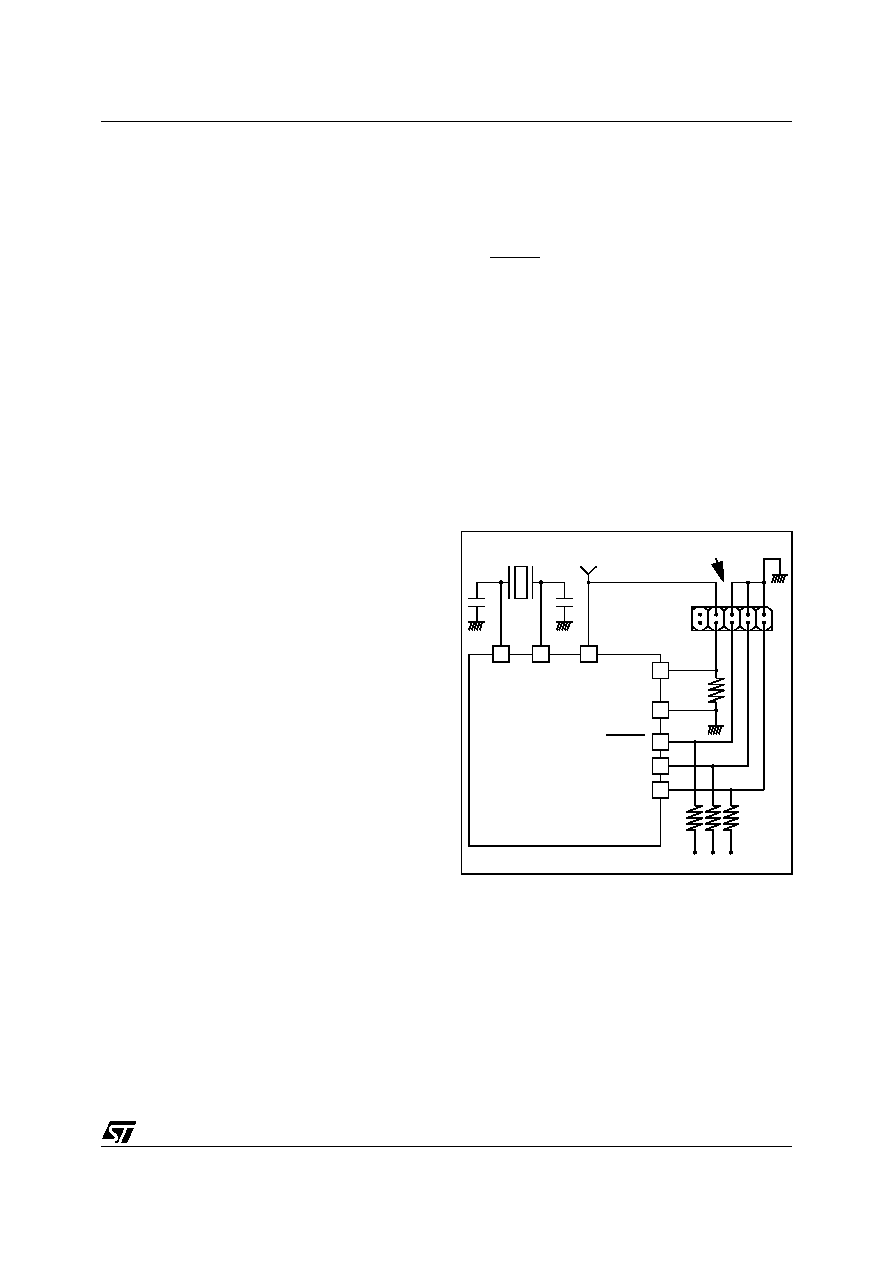
Figure 6 shows a typical hardware interface to a
standard ST7 programming tool. For more details
on the pin locations, refer to the device pinout de-
scription.
Figure 6. Typical Remote ISP Interface
5.5 MEMORY READ-OUT PROTECTION
The read-out protection is enabled through an op-
tion bit.
For FLASH devices, when this option is selected,
the program and data stored in the FLASH memo-
ry are protected against read-out piracy (including
a re-write protection). When this protection option
is removed the entire FLASH program memory is
first automatically erased. However, the E2PROM
data memory (when available) can be protected
only with ROM devices.
ISPSEL
VSS
RESET
ISPCLK
ISPDATA
OS
C
1
OS
C
2
V
DD
ST7
HE10 CONNECTOR TYPE
TO PROGRAMMING TOOL
10K
CL0
CL1
APPLICATION
47K
1
XTAL
相關(guān)PDF資料 |
PDF描述 |
|---|---|
| ST72C124J4T6 | IC-ST7 MICROCONTROLLER |
| ST72C314J2 | 8-BIT MCU WITH SINGLE VOLTAGE FLASH MEMORY. ADC. 16-BIT TIMERS. SPI. SCI INTERFACES |
| ST72C314J4 | CMOS Image Sensor |
| ST72C314N2 | CMOS Image Sensor |
| ST72C314N4 | CMOS Image Sensor |
相關(guān)代理商/技術(shù)參數(shù) |
參數(shù)描述 |
|---|---|
| ST72C124J4T6 | 制造商:STMicroelectronics 功能描述: |
| ST72C171K2B6 | 功能描述:8位微控制器 -MCU Flash 8K SPI/SCI RoHS:否 制造商:Silicon Labs 核心:8051 處理器系列:C8051F39x 數(shù)據(jù)總線寬度:8 bit 最大時鐘頻率:50 MHz 程序存儲器大小:16 KB 數(shù)據(jù) RAM 大小:1 KB 片上 ADC:Yes 工作電源電壓:1.8 V to 3.6 V 工作溫度范圍:- 40 C to + 105 C 封裝 / 箱體:QFN-20 安裝風(fēng)格:SMD/SMT |
| ST72C171K2M6 | 功能描述:8位微控制器 -MCU Flash 8K SPI/SCI RoHS:否 制造商:Silicon Labs 核心:8051 處理器系列:C8051F39x 數(shù)據(jù)總線寬度:8 bit 最大時鐘頻率:50 MHz 程序存儲器大小:16 KB 數(shù)據(jù) RAM 大小:1 KB 片上 ADC:Yes 工作電源電壓:1.8 V to 3.6 V 工作溫度范圍:- 40 C to + 105 C 封裝 / 箱體:QFN-20 安裝風(fēng)格:SMD/SMT |
| ST72C215G2B6 | 功能描述:8位微控制器 -MCU Flash 8K SPI RoHS:否 制造商:Silicon Labs 核心:8051 處理器系列:C8051F39x 數(shù)據(jù)總線寬度:8 bit 最大時鐘頻率:50 MHz 程序存儲器大小:16 KB 數(shù)據(jù) RAM 大小:1 KB 片上 ADC:Yes 工作電源電壓:1.8 V to 3.6 V 工作溫度范圍:- 40 C to + 105 C 封裝 / 箱體:QFN-20 安裝風(fēng)格:SMD/SMT |
| ST72C215G2M3 | 制造商:STMicroelectronics 功能描述:MCU 8-Bit ST7 CISC 8KB Flash 3.3V/5V 28-Pin SO Tube 制造商:STMicroelectronics 功能描述:MCU 8BIT ST7 CISC 8KB FLASH 3.3V/5V 28SOIC - Rail/Tube |
發(fā)布緊急采購,3分鐘左右您將得到回復(fù)。