- 您現(xiàn)在的位置:買賣IC網(wǎng) > PDF目錄98142 > SST55VD020-60-C-MVWE (SILICON STORAGE TECHNOLOGY INC) IDE COMPATIBLE, FLASH MEMORY DRIVE CONTROLLER, PBGA85 PDF資料下載
參數(shù)資料
| 型號(hào): | SST55VD020-60-C-MVWE |
| 廠商: | SILICON STORAGE TECHNOLOGY INC |
| 元件分類: | 存儲(chǔ)控制器/管理單元 |
| 英文描述: | IDE COMPATIBLE, FLASH MEMORY DRIVE CONTROLLER, PBGA85 |
| 封裝: | 6 X 6 MM, ROHS COMPLIANT, MO-225, VFBGA-85 |
| 文件頁數(shù): | 43/45頁 |
| 文件大小: | 666K |
| 代理商: | SST55VD020-60-C-MVWE |
第1頁第2頁第3頁第4頁第5頁第6頁第7頁第8頁第9頁第10頁第11頁第12頁第13頁第14頁第15頁第16頁第17頁第18頁第19頁第20頁第21頁第22頁第23頁第24頁第25頁第26頁第27頁第28頁第29頁第30頁第31頁第32頁第33頁第34頁第35頁第36頁第37頁第38頁第39頁第40頁第41頁第42頁當(dāng)前第43頁第44頁第45頁
Data Sheet
NAND Controller
SST55VD020
2009 Silicon Storage Technology, Inc.
S71355-03-000
07/09
7
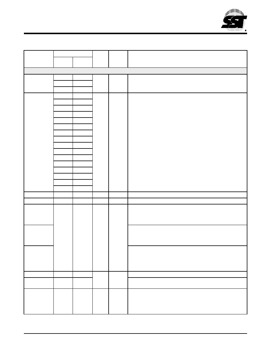
TABLE
1: Pin Assignments (1 of 4)
Symbol
Pin No.
Pin
Type
I/O
Type1
Name and Functions
100-
TQFP
85-
VFBGA
Host Side Interface
A2
53
B2
I
I1Z
A[2:0] are used to select one of eight registers in the Task File.
A1
22
D9
A0
23
D8
D15
65
D3
I/O
I1Z/O2
D[15:0] Data bus
D14
66
E2
D13
67
E3
D12
68
F2
D11
70
F3
D10
71
G1
D9
72
G2
D8
73
G3
D7
3
J9
D6
4
H10
D5
5
H9
D4
6
H8
D3
8
G9
D2
9
G8
D1
10
F10
D0
11
F9
DMACK
20
E8
I
I2U
DMA Acknowledge - input from host
DMARQ
14
F8
O
O1
DMA Request to host
IORDY
62
D2
O
O1
IORDY: When Ultra DMA mode DMA Write is not active and the
device is not ready to respond to a data transfer request, this sig-
nal is negated to extend the Host transfer cycle. However, it is
never negated by this controller.
DDMARDY#
DDMARDY#: When Ultra DMA mode DMA Write is active, this sig-
nal is asserted by the host to indicate that the device is read to
receive Ultra DMA data-in bursts. The device may negate
DDMARDY# to pause an Ultra DMA transfer.
DSTROBE
DSTROBE: When Ultra DMA mode DMA Write is active, this sig-
nal is the data-out strobe generated by the device. Both the rising
and falling edges of DSTROBE cause data to be latched by the
host. The device may stop generating DSTROBE edges to pause
an Ultra DMA data-out burst.
CS1FX#
24
C10
II2Z
CS1FX# is the chip select for the task file registers
CS3FX#
52
B1
CS3FX# is used to select the Alternate Status register and the
Device Control register.
CSEL
56
C3
I
I1U
This internally pulled-up signal is used to configure this device as a
Master or a Slave. When this pin is grounded, this device is config-
ured as a Master. When the pin is open, or tied to VDDQ, this
device is configured as a Slave. The pin setting should remain the
same from Power-on to Power-down.
相關(guān)PDF資料 |
PDF描述 |
|---|---|
| SST55VD020-60-I-TQWE | IDE COMPATIBLE, FLASH MEMORY DRIVE CONTROLLER, PQFP100 |
| SST85LD0512-60-RI-LBTE | IDE COMPATIBLE, FLASH MEMORY DRIVE CONTROLLER, PBGA91 |
| SST85LD1001T-60-RI-LBTE | IDE COMPATIBLE, FLASH MEMORY DRIVE CONTROLLER, PBGA91 |
| SST85LD1004T-60-RI-LBTE | IDE COMPATIBLE, FLASH MEMORY DRIVE CONTROLLER, PBGA91 |
| SST85LD1008M-60-PC-LBTE | IDE COMPATIBLE, FLASH MEMORY DRIVE CONTROLLER, PBGA91 |
相關(guān)代理商/技術(shù)參數(shù) |
參數(shù)描述 |
|---|---|
| SST55VD020-60-C-TQWE | 功能描述:閃存 ATA Media 60MHz 2.7V Commercial RoHS:否 制造商:ON Semiconductor 數(shù)據(jù)總線寬度:1 bit 存儲(chǔ)類型:Flash 存儲(chǔ)容量:2 MB 結(jié)構(gòu):256 K x 8 定時(shí)類型: 接口類型:SPI 訪問時(shí)間: 電源電壓-最大:3.6 V 電源電壓-最小:2.3 V 最大工作電流:15 mA 工作溫度:- 40 C to + 85 C 安裝風(fēng)格:SMD/SMT 封裝 / 箱體: 封裝:Reel |
| SST55VD020-60-I-MVWE | 功能描述:總線收發(fā)器 ATA Media 60MHz 3.3V Industrial RoHS:否 制造商:Fairchild Semiconductor 邏輯類型:CMOS 邏輯系列:74VCX 每芯片的通道數(shù)量:16 輸入電平:CMOS 輸出電平:CMOS 輸出類型:3-State 高電平輸出電流:- 24 mA 低電平輸出電流:24 mA 傳播延遲時(shí)間:6.2 ns 電源電壓-最大:2.7 V, 3.6 V 電源電壓-最小:1.65 V, 2.3 V 最大工作溫度:+ 85 C 封裝 / 箱體:TSSOP-48 封裝:Reel |
| SST55VD020-60-I-TQWE | 功能描述:閃存 ATA Media 60MHz 3.3V Industrial RoHS:否 制造商:ON Semiconductor 數(shù)據(jù)總線寬度:1 bit 存儲(chǔ)類型:Flash 存儲(chǔ)容量:2 MB 結(jié)構(gòu):256 K x 8 定時(shí)類型: 接口類型:SPI 訪問時(shí)間: 電源電壓-最大:3.6 V 電源電壓-最小:2.3 V 最大工作電流:15 mA 工作溫度:- 40 C to + 85 C 安裝風(fēng)格:SMD/SMT 封裝 / 箱體: 封裝:Reel |
| SST55VD020-60-I-TQWE-TM024 | 功能描述:閃存 ATA Media 60MHz 3.3V Industrial RoHS:否 制造商:ON Semiconductor 數(shù)據(jù)總線寬度:1 bit 存儲(chǔ)類型:Flash 存儲(chǔ)容量:2 MB 結(jié)構(gòu):256 K x 8 定時(shí)類型: 接口類型:SPI 訪問時(shí)間: 電源電壓-最大:3.6 V 電源電壓-最小:2.3 V 最大工作電流:15 mA 工作溫度:- 40 C to + 85 C 安裝風(fēng)格:SMD/SMT 封裝 / 箱體: 封裝:Reel |
| SST58LD008 | 制造商:SST 制造商全稱:Silicon Storage Technology, Inc 功能描述:ATA-Disk Chip |
發(fā)布緊急采購,3分鐘左右您將得到回復(fù)。