- 您現(xiàn)在的位置:買賣IC網(wǎng) > PDF目錄374930 > SSM3J115TU (Toshiba Corporation) Field-Effect Transistor Silicon P-Channel MOS Type High-Speed Switching Applications Power Management Switch Applications PDF資料下載
參數(shù)資料
| 型號(hào): | SSM3J115TU |
| 廠商: | Toshiba Corporation |
| 英文描述: | Field-Effect Transistor Silicon P-Channel MOS Type High-Speed Switching Applications Power Management Switch Applications |
| 中文描述: | 場(chǎng)效應(yīng)晶體管硅P溝道MOS型高速開關(guān)應(yīng)用電源管理開關(guān)應(yīng)用 |
| 文件頁數(shù): | 1/6頁 |
| 文件大小: | 145K |
| 代理商: | SSM3J115TU |
SSM3J115TU
2007-11-01
1
TOSHIBA Field-Effect Transistor Silicon P-Channel MOS Type
SSM3J115TU
High-Speed Switching Applications
Power Management Switch Applications
1.5 V drive
Low ON-resistance:
R
on
= 353 m
(max) (@V
GS
=
1.5 V)
R
on
= 193 m
(max) (@V
GS
=
1.8 V)
R
on
= 125 m
(max) (@V
GS
=
2.5 V)
R
on
= 98 m
(max) (@V
GS
=
4.0 V)
Absolute Maximum Ratings
(Ta = 25°C)
Characteristic
Symbol
Rating
Unit
Drain-source voltage
Gate-source voltage
V
DS
V
GSS
I
D
I
DP
P
D (Note 1)
P
D (Note 2)
T
ch
T
stg
20
±
8
2.2
4.4
800
500
150
55~150
V
V
DC
Pulse
Drain current
A
Drain power dissipation
mW
Channel temperature
Storage temperature range
°
C
°
C
Note:
Using continuously under heavy loads (e.g. the application of
high temperature/current/voltage and the significant change in
temperature, etc.) may cause this product to decrease in the
reliability significantly even if the operating conditions (i.e.
operating temperature/current/voltage, etc.) are within the
absolute maximum ratings.
Please design the appropriate reliability upon reviewing the
Toshiba Semiconductor Reliability Handbook (“Handling
Precautions”/“Derating Concept and Methods”) and individual
reliability data (i.e. reliability test report and estimated failure
rate, etc).
Note 1: Mounted on a ceramic board.
(25.4 mm
×
25.4 mm
×
0.8 mm, Cu Pad: 645 mm
2
)
Note 2: Mounted on an FR4 board.
(25.4 mm
×
25.4 mm
×
1.6 mm, Cu Pad: 645 mm
2
)
Electrical Characteristics
(Ta = 25°C)
Characteristic
Symbol
Test Conditions
Min
Typ.
Max
Unit
V
(BR) DSS
V
(BR) DSX
I
DSS
I
D
=
1 mA, V
GS
=
0
I
D
=
1 mA, V
GS
=
+
8 V
V
DS
=
20 V, V
GS
=
0
20
Drain-source breakdown voltage
12
V
Drain cutoff current
10
μ
A
Gate leakage current
I
GSS
V
GS
=
±
8 V, V
DS
=
0
±
1
μ
A
Gate threshold voltage
V
th
V
DS
=
3 V, I
D
=
1 mA
0.3
1.0
V
Forward transfer admittance
Y
fs
V
DS
=
3 V, I
D
=
0.9 A
(Note 3)
2.7
5.4
S
I
D
=
1.0 A, V
GS
=
4.0 V
I
D
=
1.0 A, V
GS
=
2.5 V
I
D
=
1.0 A, V
GS
=
1.8 V
I
D
=
0.1 A, V
GS
=
1.5 V
V
DS
=
10 V, V
GS
=
0, f
=
1 MHz
(Note 3)
77
98
(Note 3)
84
111
126
125
193
353
Drain-source ON-resistance
(Note 3)
m
Ω
R
DS (ON)
(Note 3)
Input capacitance
C
iss
568
pF
Output capacitance
C
oss
V
DS
=
10 V, V
GS
=
0, f
=
1 MHz
75
pF
Reverse transfer capacitance
C
rss
V
DS
=
10 V, V
GS
=
0, f
=
1 MHz
67
pF
Turn-on time
t
on
29
Switching time
Turn-off time
t
off
V
DD
=
10 V, I
D
=
0.9 A,
V
GS
=
0~
2.5 V, R
G
=
4.7
Ω
39
ns
Drain-source forward voltage
V
DSF
I
D
=
2.2 A, V
GS
=
0 V
(Note 3)
0.8
1.2
V
Note 3: Pulse test
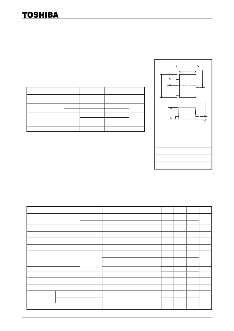
Unit: mm
JEDEC
―
JEITA
―
TOSHIBA
2-2U1A
Weight: 6.6 mg (typ.)
1: Gate
2: Source
3: Drain
UFM
-
0
1.7±0.1
2.1±0.1
0
1
2
2
3
0
+
0
相關(guān)PDF資料 |
PDF描述 |
|---|---|
| SSM3J117TU | Field-Effect Transistor Silicon P-Channel MOS Type High-Speed Switching Applications |
| SSM3J118TU | Field-Effect Transistor Silicon P-Channel MOS Type High-Speed Switching Applications |
| SSM3J120TU | Field Effect Transistor Silicon P Channel MOS Type Power Management Switch Applications High-Current Switching Applications |
| SSM3J13T | TOSHIBA Field Effect Transistor Silicon P Channel MOS Type (U-MOSII) |
| SSM3J14T | TOSHIBA Field Effect Transistor Silicon P Channel MOS Type (U-MOSII) |
相關(guān)代理商/技術(shù)參數(shù) |
參數(shù)描述 |
|---|---|
| SSM3J115TU(TE85L) | 功能描述:MOSFET Vds=-20V Id=-2.2A 3Pin RoHS:否 制造商:STMicroelectronics 晶體管極性:N-Channel 汲極/源極擊穿電壓:650 V 閘/源擊穿電壓:25 V 漏極連續(xù)電流:130 A 電阻汲極/源極 RDS(導(dǎo)通):0.014 Ohms 配置:Single 最大工作溫度: 安裝風(fēng)格:Through Hole 封裝 / 箱體:Max247 封裝:Tube |
| SSM3J115TUTE85L | 制造商:Toshiba America Electronic Components 功能描述:SMALL SIGNAL MOSFET TRANSISTOR |
| SSM3J117TU | 功能描述:MOSFET INCORRECT MOUSER P/N 3Pin RoHS:否 制造商:STMicroelectronics 晶體管極性:N-Channel 汲極/源極擊穿電壓:650 V 閘/源擊穿電壓:25 V 漏極連續(xù)電流:130 A 電阻汲極/源極 RDS(導(dǎo)通):0.014 Ohms 配置:Single 最大工作溫度: 安裝風(fēng)格:Through Hole 封裝 / 箱體:Max247 封裝:Tube |
| SSM3J117TU(TE85L) | 功能描述:MOSFET Vds=-30V Id=-2A 3Pin RoHS:否 制造商:STMicroelectronics 晶體管極性:N-Channel 汲極/源極擊穿電壓:650 V 閘/源擊穿電壓:25 V 漏極連續(xù)電流:130 A 電阻汲極/源極 RDS(導(dǎo)通):0.014 Ohms 配置:Single 最大工作溫度: 安裝風(fēng)格:Through Hole 封裝 / 箱體:Max247 封裝:Tube |
| SSM3J118TU | 功能描述:MOSFET INCORRECT MOUSER P/N 3Pin RoHS:否 制造商:STMicroelectronics 晶體管極性:N-Channel 汲極/源極擊穿電壓:650 V 閘/源擊穿電壓:25 V 漏極連續(xù)電流:130 A 電阻汲極/源極 RDS(導(dǎo)通):0.014 Ohms 配置:Single 最大工作溫度: 安裝風(fēng)格:Through Hole 封裝 / 箱體:Max247 封裝:Tube |
發(fā)布緊急采購,3分鐘左右您將得到回復(fù)。