- 您現(xiàn)在的位置:買賣IC網 > PDF目錄297426 > SPT8000SIT (FAIRCHILD SEMICONDUCTOR CORP) 1-CH 14-BIT FLASH METHOD ADC, PARALLEL ACCESS, PQFP44 PDF資料下載
參數(shù)資料
| 型號: | SPT8000SIT |
| 廠商: | FAIRCHILD SEMICONDUCTOR CORP |
| 元件分類: | ADC |
| 英文描述: | 1-CH 14-BIT FLASH METHOD ADC, PARALLEL ACCESS, PQFP44 |
| 封裝: | PLASTIC, TQFP-44 |
| 文件頁數(shù): | 3/11頁 |
| 文件大小: | 130K |
| 代理商: | SPT8000SIT |
11
10/12/01
SPT8000
ORDERING INFORMATION
PART NUMBER
TEMPERATURE RANGE
PACKAGE
SPT8000SIT
–40 to +85 °C
44L TQFP
remains High until it completes the calibration. The
internal calibration routine takes approximately
74.5 ms for 20 MHz clock input. The SPT8000
ignores the Analog Input when BUSY is High.
When BUSY is Low, it is ready to convert the
Analog Input.
CAL
Calibration Start Input. Holding CAL High for more
than two falling edges of CLK, while RESETB is
High, initiates the SPT8000’s internal calibration
routine.
RESETB
Reset Input (active Low). Logic 0 on this
asynchronous reset pin will set the internal digital
state machine to its initial state and clear all
internal calibration coefficients.
VBS
Noise Reduction Pin. Connect a noise reduction
capacitor of 4.7 F or larger from this pin to
AGND.
CM
Common Mode Level Output. +2.25 V nominal.
Connect a noise reduction capacitor of 4.7 F or
larger from this pin to AGND.
VRC
Lower Reference. +1.25 V nominal. This voltage
sets the lower bound of analog input span.
Connect a noise reduction capacitor of 4.7 F or
larger from this pin to AGND.
VRT
Upper Reference. +3.25 V nominal. This voltage
sets the upper bound of analog input span.
Connect a noise reduction capacitor of 4.7 F or
larger from this pin to AGND.
VIN+
Analog Input Pin (+). The nominal span at this pin
is +1.25 V to +3.25 V.
VIN–
Analog Input Pin (–). The nominal span at this pin
is +3.25 V to +1.25 V.
VREF/EXTB Voltage Reference I/O Pin. +1.00 V nominal. The
voltage at this pin sets the span above and below
CM for each analog input pin. Driving VREF/EXTB
to 0 V will disable internal buffers driving VRT and
VRC, allowing the user to drive VRT and VRC
externally. Connect a noise reduction capacitor of
4.7 F or larger from this pin to AGND.
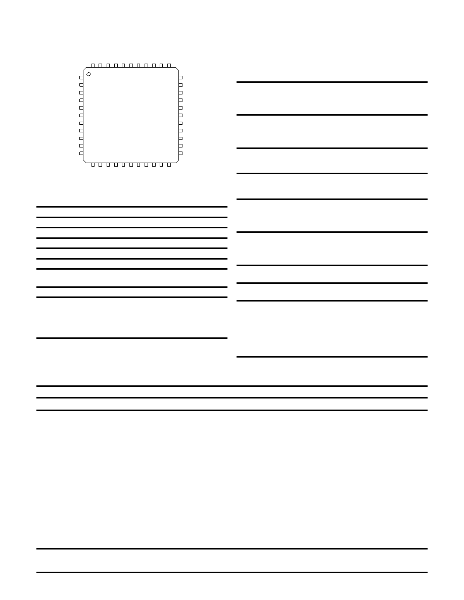
PIN ASSIGNMENTS
12
13
14
15
16
17
18
19
20
21
22
44
43
42
41
40
39
38
37
36
35
34
1
2
3
4
5
6
7
8
9
10
11
33
32
31
30
29
28
27
26
25
24
23
AGND
BGND
N/C
AVDD
AGND
AVDD
CLK
D0 (LSB)
D1
D2
D3
D4
D5
D6
D7
D8
D9
D10
D1
1
AGND
N/C
BGND
AVDD
CAL
BUSY
OTR
D13 (MSB)
D12
V
REF
/EXTB
N/C
V
IN
V
IN
+
N/C
V
RT
V
RC
N/C
V
BS
AVDD
OGND
OVDD
RESETB
AVDD
CM
N/C
SPT8000
PIN FUNCTIONS
Name
Description
AGND
Ground
AVDD
+5 V Supply
N/C
No Connect. Leave the pin open or tie it to AGND.
BGND
Ground
CLK
Clock Input
OGND
Ground for BUSY, OTR, and Data Bit Outputs
OVDD
+3.3 V to +5 V Supply for BUSY, OTR, and Data
Bit Outputs
D0–D13
Data Bit Outputs. D0=LSB, D13=MSB
OTR
Out of Range Output. OTR goes High for the
Analog input above (overrange) or below
(underrange) the full-scale range. The
corresponding Data Bit Outputs are all 1s for
overrange, and all 0s for underrange.
BUSY
Busy Output. BUSY goes High when the SPT8000
goes into its internal calibration routine and
LIFE SUPPORT POLICY
FAIRCHILD'S PRODUCTS ARE NOT AUTHORIZED FOR USE AS CRITICAL COMPONENTS IN LIFE SUPPORT DEVICES OR SYSTEMS
WITHOUT THE EXPRESS WRITTEN APPROVAL OF THE PRESIDENT OF FAIRCHILD SEMICONDUCTOR CORPORATION. As used herein:
1. Life support devices or systems are devices or systems which, (a) are
intended for surgical implant into the body, or (b) support or sustain life,
and whose failure to perform, when properly used in accordance with
instructions for use provided in the labeling, can be reasonably
expected to result in a significant injury to the user.
2. A critical component is any component of a life support device or
system whose failure to perform can be reasonably expected to cause
the failure of the life support device or system, or to affect its safety or
effectiveness.
DISCLAIMER
FAIRCHILD SEMICONDUCTOR RESERVES THE RIGHT TO MAKE CHANGES WITHOUT FURTHER NOTICE TO ANY PRODUCTS HEREIN TO
IMPROVE RELIABILITY, FUNCTION OR DESIGN. FAIRCHILD DOES NOT ASSUME ANY LIABILITY ARISING OUT OF THE APPLICATION OR
USE OF ANY PRODUCT OR CIRCUIT DESCRIBED HEREIN; NEITHER DOES IT CONVEY ANY LICENSE UNDER ITS PATENT RIGHTS, NOR
THE RIGHTS OF OTHERS.
www.fairchildsemi.com
Copyright 2002 Fairchild Semiconductor Corporation
相關PDF資料 |
PDF描述 |
|---|---|
| SPT9712AIN | PARALLEL, WORD INPUT LOADING, 0.013 us SETTLING TIME, 12-BIT DAC, PDIP28 |
| SPT9712BIN | PARALLEL, WORD INPUT LOADING, 0.013 us SETTLING TIME, 12-BIT DAC, PDIP28 |
| SPX-2000 | INDUSTRY LEADERS DEPEND ON US ...FOR SOLUTIONS |
| SPX1083AU-L | 1.2 V-ADJUSTABLE POSITIVE LDO REGULATOR, 1.2 V DROPOUT, PSFM3 |
| SPX1083AU-L-3.3 | 3.3 V FIXED POSITIVE LDO REGULATOR, 1.2 V DROPOUT, PSFM3 |
相關代理商/技術參數(shù) |
參數(shù)描述 |
|---|---|
| SPT8100 | 制造商:FAIRCHILD 制造商全稱:Fairchild Semiconductor 功能描述:16-BIT, 5 MSPS CMOS A/D CONVERTER |
| SPT8100SIT | 功能描述:模數(shù)轉換器 - ADC 16-Bit 5 MSPS CMOS ADC RoHS:否 制造商:Texas Instruments 通道數(shù)量:2 結構:Sigma-Delta 轉換速率:125 SPs to 8 KSPs 分辨率:24 bit 輸入類型:Differential 信噪比:107 dB 接口類型:SPI 工作電源電壓:1.7 V to 3.6 V, 2.7 V to 5.25 V 最大工作溫度:+ 85 C 安裝風格:SMD/SMT 封裝 / 箱體:VQFN-32 |
| SPT8100SIT_Q | 功能描述:模數(shù)轉換器 - ADC 16-Bit 5 MSPS CMOS ADC RoHS:否 制造商:Texas Instruments 通道數(shù)量:2 結構:Sigma-Delta 轉換速率:125 SPs to 8 KSPs 分辨率:24 bit 輸入類型:Differential 信噪比:107 dB 接口類型:SPI 工作電源電壓:1.7 V to 3.6 V, 2.7 V to 5.25 V 最大工作溫度:+ 85 C 安裝風格:SMD/SMT 封裝 / 箱體:VQFN-32 |
| SPT8102PDK | 功能描述:開發(fā)板和工具包 - 其他處理器 8102 PDK KIT RoHS:否 制造商:Freescale Semiconductor 產品:Development Systems 工具用于評估:P3041 核心:e500mc 接口類型:I2C, SPI, USB 工作電源電壓: |
| SPT8102PFC | 功能描述:子卡和OEM板 MSC8102 FARM CARD FOR PD RoHS:否 制造商:BeagleBoard by CircuitCo 產品:BeagleBone LCD4 Boards 用于:BeagleBone - BB-Bone - Open Source Development Kit |
發(fā)布緊急采購,3分鐘左右您將得到回復。