- 您現(xiàn)在的位置:買賣IC網(wǎng) > PDF目錄385856 > SP8126B High Speed Differential APC Amplifier PDF資料下載
參數(shù)資料
| 型號: | SP8126B |
| 英文描述: | High Speed Differential APC Amplifier |
| 中文描述: | apc的高速差分放大器 |
| 文件頁數(shù): | 3/8頁 |
| 文件大小: | 91K |
| 代理商: | SP8126B |
3
Rev:B Date: 3/18/04
SP8126B High Speed Differential APC Amplifier
Copyright 2004 Sipex Corporation
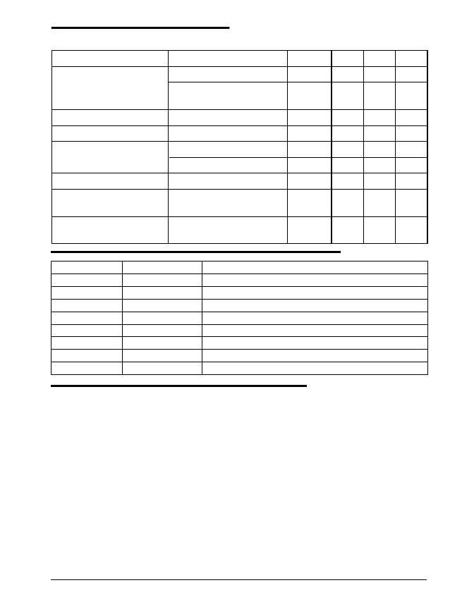
PIN DESCRIPTION
PIN NUMBER
1
2
3
4
5
6
7
8
NAME
V
CC
GAIN
R
GCOM
GND
R
GAIN1
R
GAIN2
V
OUT
-
V
OUT
+
FUNCTION
Supply Voltage
Gain Select
Common connection point for R
GAIN
1 and R
GAIN
2
Power Ground
Gain Adjust 1 (Gain Select = LOW) or OPEN
Gain Adjust 2 (Gain Select = HIGH)
Output Voltage -
Output Voltage +
Internal Operation
The SP8126B APC circuit has an integrated
photo detector and is designed with nominal
sensitivities of 3mV/
μ
W for both 650nm and
780nm wavelength laser light. The part's sensi-
tivity can also be adjusted continuously and
independently for two different gain modes via
two external resistors over a range of
±
6dB. The
two gain modes are controlled by a TTL com-
patible logic input, called GAIN SELECT. This
logic pin selects between the two external gain
setting resistors to allow independent control
and settings for the two gain functions.
The system is a two stage design, consisting of
a Trans-Impedance Amplifier (TIA) and an out-
put buffer stage. In dark condition the outputs
V
OUT
- and V
OUT
+ are set to a reference voltage
that is defined internally as Vcc/2. With 650nm
or 780nm wavelength laser light falling on the
photodetector, the output will swing differen-
tially around Vcc/2 proportional with the light
power according to the chosen gain.
TIA and Gain control
The first stage is a differential TIA used to
convert the photodetector current to a balanced
differential voltage. The traditional fixed feed-
back resistors have been replaced with an active
resistor circuit that sets the trans-impedance value.
A Resistor Control Block that senses the value
of the external gain setting resistor controls the
value of the equivalent feedback resistor.
PARAMETER
CONDITIONS
MIN
TYP
MAX
UNITS
Output Settling Time (780nm)
2V
PP
Step
10
13
ns
(1% of Final Value)
2V
PP
Step,
R
GAIN
= 1230
(High Gain)
15
18
ns
Output Slew Rate
200
300
V/
μ
s
Output Overshoot
2V
PP
Step
5
%
Power Supply Current
15
mA
-20
°
C < T
A
< +85
°
C
20
mA
Gain Adjust Range
225
< R
GAIN
< 1230
-6
6
dB
Gain Select Input Voltage
VIL (TTL Level)
0.8
V
Gain Select Input Voltage
VIH (TTL Level)
2.0
V
THEORY OF OPERATION
Unless otherwise noted: V
CC
= 5.0V, C
LOAD
= 50pF to GND, R
LOADP
= R
LOADN
= 1k
to GND, R
GAIN
= 510
(Nominal Gain), -20
°
C
≤
T
A
≤
+85
°
C, Output measured differentially.
ELECTRICAL SPECIFICATIONS: Continued
相關(guān)PDF資料 |
PDF描述 |
|---|---|
| SP8127 | High Speed Differential APC Amplifier |
| SP8127DG | High Speed Differential APC Amplifier |
| SP8130 | High Speed Differential APC Amplifier |
| SP8130DG4 | High Speed Differential APC Amplifier |
| SP9501 | 12-Bit, Voltage Output D/A Converter |
相關(guān)代理商/技術(shù)參數(shù) |
參數(shù)描述 |
|---|---|
| SP8126CB-3 | 制造商:SIPEX 制造商全稱:Sipex Corporation 功能描述:High Speed Differential APC Amplifier |
| SP8127 | 制造商:SIPEX 制造商全稱:Sipex Corporation 功能描述:High Speed Differential APC Amplifier |
| SP8127DG | 制造商:SIPEX 制造商全稱:Sipex Corporation 功能描述:High Speed Differential APC Amplifier |
| SP8127N | 制造商:SIPEX 制造商全稱:Sipex Corporation 功能描述:High Speed Differential APC Amplifier |
| SP8127NDG | 制造商:SIPEX 制造商全稱:Sipex Corporation 功能描述:High Speed Differential APC Amplifier |
發(fā)布緊急采購,3分鐘左右您將得到回復(fù)。