- 您現在的位置:買賣IC網 > PDF目錄26899 > SP8042EW LINEAR OUTPUT PHOTO DETECTOR PDF資料下載
參數資料
| 型號: | SP8042EW |
| 元件分類: | 光電元器件 |
| 英文描述: | LINEAR OUTPUT PHOTO DETECTOR |
| 文件頁數: | 2/4頁 |
| 文件大小: | 46K |
| 代理商: | SP8042EW |
2
Rev. 8/19/03
SP8042 7 Channel, PDIC
Copyright 2003 Sipex Corporation
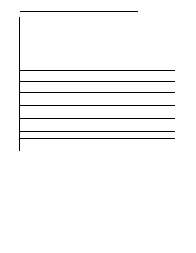
PIN DESCRIPTION
PIN No.
NAME
DESCRIPTION
1Bb
Output of Bb channel (B or b sensor output depending upon SW
position).
2Aa
Output of Aa channel (A or a sensor output depending upon SW
position).
3SW
Mode switch input. High logic level selects CD mode, low - DVD mode.
4RF
Output of RF channel. RF = A + B + C + D or RF = a + b + v + d
depending upon SW position.
5NC
No Connection.
6Dd
Output of Dd channel (D or d sensor output depending upon SW
position.
7Cc
Output of Cc channel (C or c sensor output depending upon SW
position)
8NC
No Connection.
9
GND
Ground Pin.
10
F
Output of F Channel.
11
NC
No Connection.
12
VS
Reference Voltage. Bypass to GND with ceramic capacitor 0.1
F.
13
VCC
Supply Voltage. Bypass to GND with ceramic capacitor 0.1
F.
14
E
Output of E Channel.
15
NC
No Connection.
16
GND
Ground Pin.
BOARD LAYOUT AND GROUNDING
To obtain the best performance from the SP8042, a printed circuit board with ground plane is required.
Both ground pins (pins #9 and #16) should be connected to the ground plane. High quality, low series
resistance ceramic 0.1
F bypass capacitors should be used at the V
CC and VS pins (pins 12 and 13).
These capacitors must be located as close to the pins as possible.
The traces connection the pins to the ground plane, VCC, VS, and bypassing capacitors must be kept
short and should be made as wide as possible.
相關PDF資料 |
PDF描述 |
|---|---|
| SP8062DG | LOGIC OUTPUT PHOTO DETECTOR |
| SP8062DG-L | LOGIC OUTPUT PHOTO DETECTOR |
| SPD1511-18-11 | PIN PHOTO DIODE |
| SPD9441TX | PHOTO DIODE |
| SPD9441SMSTX | PHOTO DIODE |
相關代理商/技術參數 |
參數描述 |
|---|---|
| SP8042PB | 制造商:SIPEX 制造商全稱:Sipex Corporation 功能描述:7 Channel Photo Detector IC |
| SP8042W | 制造商:SIPEX 制造商全稱:Sipex Corporation 功能描述:7 Channel Photo Detector IC |
| SP8043 | 制造商:SIPEX 制造商全稱:Sipex Corporation 功能描述:10 Channel Photo Detector IC |
| SP8043DC | 制造商:SIPEX 制造商全稱:Sipex Corporation 功能描述:10 Channel Photo Detector IC |
| SP8043DG1 | 制造商:SIPEX 制造商全稱:Sipex Corporation 功能描述:10 Channel Photo Detector IC |
發(fā)布緊急采購,3分鐘左右您將得到回復。