- 您現(xiàn)在的位置:買賣IC網(wǎng) > PDF目錄98095 > SNJ54AHC244WR (TEXAS INSTRUMENTS INC) AHC/VHC/H/U/V SERIES, DUAL 4-BIT DRIVER, TRUE OUTPUT, CDFP20 PDF資料下載
參數(shù)資料
| 型號: | SNJ54AHC244WR |
| 廠商: | TEXAS INSTRUMENTS INC |
| 元件分類: | 總線收發(fā)器 |
| 英文描述: | AHC/VHC/H/U/V SERIES, DUAL 4-BIT DRIVER, TRUE OUTPUT, CDFP20 |
| 封裝: | HERMETIC SEALED, CERAMIC, FP-20 |
| 文件頁數(shù): | 12/23頁 |
| 文件大小: | 802K |
| 代理商: | SNJ54AHC244WR |
SN54AHC244, SN74AHC244
OCTAL BUFFERS/DRIVERS
WITH 3-STATE OUTPUTS
SCLS226J OCTOBER 1995 REVISED JULY 2003
2
POST OFFICE BOX 655303
DALLAS, TEXAS 75265
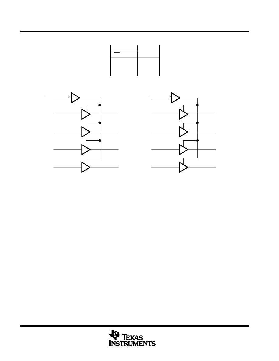
FUNCTION TABLE
(each 4-bit buffer/driver)
INPUTS
OUTPUT
OE
A
OUTPUT
Y
L
H
L
LL
H
X
Z
logic diagram (positive logic)
1
218
1Y1
1OE
1A1
416
1Y2
1A2
614
1Y3
1A3
812
1Y4
1A4
19
11
9
2Y1
2OE
2A1
13
7
2Y2
2A2
15
5
2Y3
2A3
17
3
2Y4
2A4
absolute maximum ratings over operating free-air temperature range (unless otherwise noted)
Supply voltage range, VCC
0.5 V to 7 V
. . . . . . . . . . . . . . . . . . . . . . . . . . . . . . . . . . . . . . . . . . . . . . . . . . . . . . . . . .
Input voltage range, VI (see Note 1)
0.5 V to 7 V
. . . . . . . . . . . . . . . . . . . . . . . . . . . . . . . . . . . . . . . . . . . . . . . . . .
Output voltage range, VO (see Note 1)
0.5 V to VCC + 0.5 V
. . . . . . . . . . . . . . . . . . . . . . . . . . . . . . . . . . . . . . . . .
Input clamp current, IIK (VI < 0)
20 mA
. . . . . . . . . . . . . . . . . . . . . . . . . . . . . . . . . . . . . . . . . . . . . . . . . . . . . . . . . . .
Output clamp current, IOK (VO < 0 or VO > VCC)
±20 mA
. . . . . . . . . . . . . . . . . . . . . . . . . . . . . . . . . . . . . . . . . . . . .
Continuous output current, IO (VO = 0 to VCC)
±25 mA
. . . . . . . . . . . . . . . . . . . . . . . . . . . . . . . . . . . . . . . . . . . . . . .
Continuous current through VCC or GND
±50 mA
. . . . . . . . . . . . . . . . . . . . . . . . . . . . . . . . . . . . . . . . . . . . . . . . . . .
Package thermal impedance,
θJA (see Note 2): DB package
70
°C/W
. . . . . . . . . . . . . . . . . . . . . . . . . . . . . . . . .
DGV package
92
°C/W
. . . . . . . . . . . . . . . . . . . . . . . . . . . . . . . .
DW package
58
°C/W
. . . . . . . . . . . . . . . . . . . . . . . . . . . . . . . . .
N package
69
°C/W
. . . . . . . . . . . . . . . . . . . . . . . . . . . . . . . . . . .
NS package
60
°C/W
. . . . . . . . . . . . . . . . . . . . . . . . . . . . . . . . .
PW package
83
°C/W
. . . . . . . . . . . . . . . . . . . . . . . . . . . . . . . . .
Storage temperature range, Tstg
65
°C to 150°C
. . . . . . . . . . . . . . . . . . . . . . . . . . . . . . . . . . . . . . . . . . . . . . . . . . .
Stresses beyond those listed under “absolute maximum ratings” may cause permanent damage to the device. These are stress ratings only, and
functional operation of the device at these or any other conditions beyond those indicated under “recommended operating conditions” is not
implied. Exposure to absolute-maximum-rated conditions for extended periods may affect device reliability.
NOTES:
1. The input and output voltage ratings may be exceeded if the input and output current ratings are observed.
2. The package thermal impedance is calculated in accordance with JESD 51-7.
相關(guān)PDF資料 |
PDF描述 |
|---|---|
| SN74AHC245DBRG4 | AHC/VHC/H/U/V SERIES, 8-BIT TRANSCEIVER, TRUE OUTPUT, PDSO20 |
| SN74AHC245DBLE | AHC SERIES, 8-BIT TRANSCEIVER, TRUE OUTPUT, PDSO20 |
| SNJ54AHC245J | AHC SERIES, 8-BIT TRANSCEIVER, TRUE OUTPUT, CDIP20 |
| SN74AHC245DWE4 | AHC SERIES, 8-BIT TRANSCEIVER, TRUE OUTPUT, PDSO20 |
| SN74AHC245PWLE | AHC SERIES, 8-BIT TRANSCEIVER, TRUE OUTPUT, PDSO20 |
相關(guān)代理商/技術(shù)參數(shù) |
參數(shù)描述 |
|---|---|
| SNJ54AHC245FK | 制造商:Texas Instruments 功能描述:Bus XCVR Single 8-CH 3-ST 20-Pin LCCC Tube |
| SNJ54AHC245J | 制造商:Texas Instruments 功能描述: |
| SNJ54AHC245W | 制造商:TI 制造商全稱:Texas Instruments 功能描述:OCTAL BUS TRANSCEIVERS WITH 3-STATE OUTPUTS |
| SNJ54AHC273FK | 制造商:Texas Instruments 功能描述:Flip Flop D-Type Bus Interface Pos-Edge 1-Element 20-Pin LCCC Tube |
| SNJ54AHC273J | 制造商:Texas Instruments 功能描述:5962-9853001QRA, OCTAL D-TYPE FF W/CLR - Rail/Tube 制造商:Texas Instruments 功能描述:Flip Flop D-Type Bus Interface Pos-Edge 1-Element 20-Pin CDIP Tube |
發(fā)布緊急采購,3分鐘左右您將得到回復(fù)。