- 您現(xiàn)在的位置:買賣IC網(wǎng) > PDF目錄98125 > SN74LVC3G34DCTRE4 (TEXAS INSTRUMENTS INC) LVC/LCX/Z SERIES, TRIPLE 1-INPUT NON-INVERT GATE, PDSO8 PDF資料下載
參數(shù)資料
| 型號: | SN74LVC3G34DCTRE4 |
| 廠商: | TEXAS INSTRUMENTS INC |
| 元件分類: | 門電路 |
| 英文描述: | LVC/LCX/Z SERIES, TRIPLE 1-INPUT NON-INVERT GATE, PDSO8 |
| 封裝: | GREEN, PLASTIC, SSOP-8 |
| 文件頁數(shù): | 1/13頁 |
| 文件大小: | 522K |
| 代理商: | SN74LVC3G34DCTRE4 |
www.ti.com
FEATURES
Seemechanicaldrawingsfordimensions.
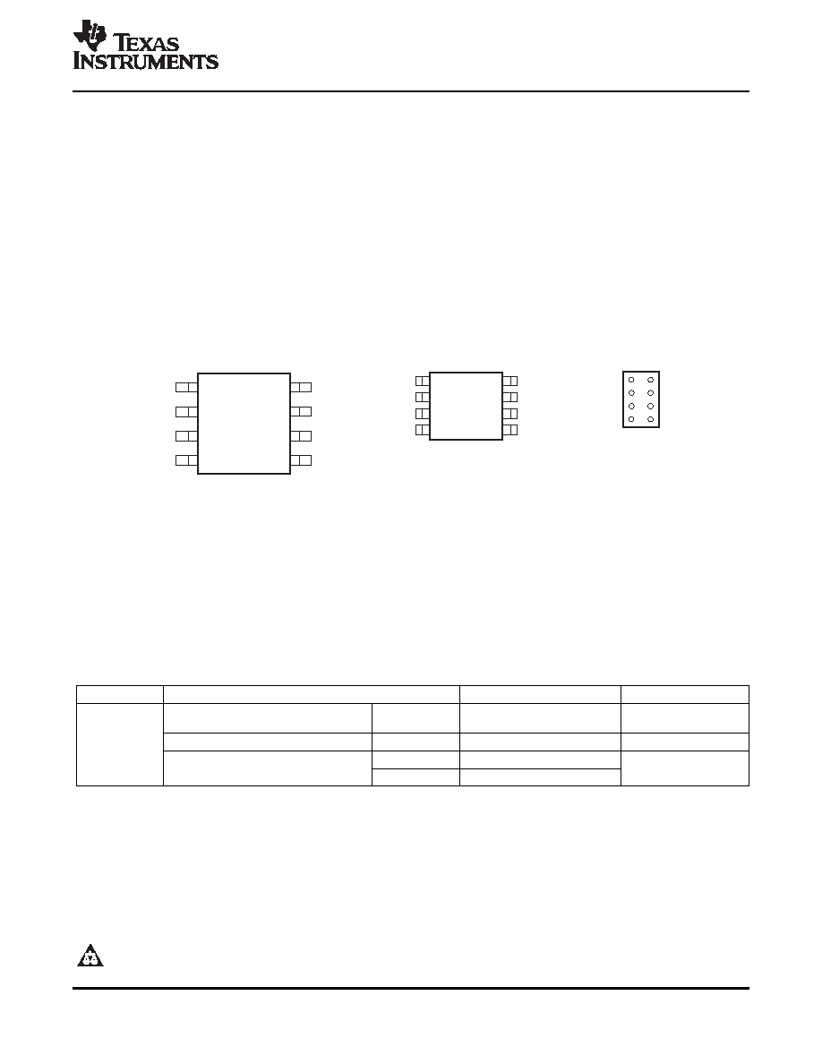
DCTPACKAGE
(TOP VIEW)
DCUPACKAGE
(TOP VIEW)
YZP PACKAGE
(BOTTOMVIEW)
1
V
CC
8
1A
2
7
3Y
1Y
3
6
2A
3A
4
5
GND
2Y
3
6
3A
2A
8
1
V
CC
1A
5
GND
4
2Y
2
7
1Y
3Y
GND
5
4
2Y
3 6
3A
2A
2 7
1Y
3Y
8
V
CC
1
1A
DESCRIPTION/ORDERING INFORMATION
TRIPLE BUFFER GATE
SCES366J – AUGUST 2001 – REVISED FEBRUARY 2007
Available in the Texas Instruments
I
off Supports Partial-Power-Down Mode
NanoFree Package
Operation
Supports 5-V V
CC Operation
Latch-Up Performance Exceeds 100 mA Per
JESD 78, Class II
Inputs Accept Voltages to 5.5 V
ESD Protection Exceeds JESD 22
Max t
pd of 4.1 ns at 3.3 V
–
2000-V Human-Body Model (A114-A)
Low Power Consumption, 10-A Max I
CC
–
200-V Machine Model (A115-A)
±24-mA Output Drive at 3.3 V
–
1000-V Charged-Device Model (C101)
Typical V
OLP (Output Ground Bounce)
<0.8 V at V
CC = 3.3 V, TA = 25°C
Typical V
OHV (Output VOH Undershoot)
>2 V at V
CC = 3.3 V, TA = 25°C
This triple buffer gate is designed for 1.65-V to 5.5-V VCC operation. The SN74LVC3G34 performs the Boolean
function Y = A in positive logic.
NanoFree package technology is a major breakthrough in IC packaging concepts, using the die as the
package.
This device is fully specified for partial-power-down applications using Ioff. The Ioff circuitry disables the outputs,
preventing damaging current backflow through the device when it is powered down.
ORDERING INFORMATION
TA
PACKAGE(1)
ORDERABLE PART NUMBER
TOP-SIDE MARKING(2)
NanoFree – WCSP (DSBGA)
Reel of 3000
SN74LVC3G34YZPR
_ _ _C9_
0.23-mm Large Bump – YZP (Pb-free)
SSOP – DCT
Reel of 3000
SN74LVC3G34DCTR
C34_ _ _
–40
°C to 85°C
Reel of 3000
SN74LVC3G34DCUR
VSSOP – DCU
C34_
Reel of 250
SN74LVC3G34DCUT
(1)
Package drawings, standard packing quantities, thermal data, symbolization, and PCB design guidelines are available at
www.ti.com/sc/package.
(2)
DCT: The actual top-side marking has three additional characters that designate the year, month, and assembly/test site.
DCU: The actual top-side marking has one additional character that designates the assembly/test site.
YZP: The actual top-side marking has three preceding characters to denote year, month, and sequence code, and one following
character to designate the assembly/test site. Pin 1 identifier indicates solder-bump composition (1 = SnPb,
= Pb-free).
Please be aware that an important notice concerning availability, standard warranty, and use in critical applications of Texas
Instruments semiconductor products and disclaimers thereto appears at the end of this data sheet.
NanoFree is a trademark of Texas Instruments.
PRODUCTION DATA information is current as of publication date.
Copyright 2001–2007, Texas Instruments Incorporated
Products conform to specifications per the terms of the Texas
Instruments standard warranty. Production processing does not
necessarily include testing of all parameters.
相關(guān)PDF資料 |
PDF描述 |
|---|---|
| SN74LVC3G34YZAR | LVC/LCX/Z SERIES, TRIPLE 1-INPUT NON-INVERT GATE, BGA8 |
| SN74LVC3G34YEPR | LVC/LCX/Z SERIES, TRIPLE 1-INPUT NON-INVERT GATE, BGA8 |
| SN74LVC3GU04YZPR | LVC/LCX/Z SERIES, TRIPLE 1-INPUT INVERT GATE, BGA8 |
| SN74LVC4245ADWG4 | LVC/LCX/Z SERIES, 8-BIT TRANSCEIVER, TRUE OUTPUT, PDSO24 |
| SN74LVC4245APWR | LVC/LCX/Z SERIES, 8-BIT TRANSCEIVER, TRUE OUTPUT, PDSO24 |
相關(guān)代理商/技術(shù)參數(shù) |
參數(shù)描述 |
|---|---|
| SN74LVC3G34DCTRG4 | 功能描述:緩沖器和線路驅(qū)動器 Triple Buffer Gate RoHS:否 制造商:Micrel 輸入線路數(shù)量:1 輸出線路數(shù)量:2 極性:Non-Inverting 電源電壓-最大:+/- 5.5 V 電源電壓-最小:+/- 2.37 V 最大工作溫度:+ 85 C 安裝風(fēng)格:SMD/SMT 封裝 / 箱體:MSOP-8 封裝:Reel |
| SN74LVC3G34DCU3 | 制造商:Texas Instruments 功能描述: |
| SN74LVC3G34DCUR | 功能描述:緩沖器和線路驅(qū)動器 Triple RoHS:否 制造商:Micrel 輸入線路數(shù)量:1 輸出線路數(shù)量:2 極性:Non-Inverting 電源電壓-最大:+/- 5.5 V 電源電壓-最小:+/- 2.37 V 最大工作溫度:+ 85 C 安裝風(fēng)格:SMD/SMT 封裝 / 箱體:MSOP-8 封裝:Reel |
| SN74LVC3G34DCUR | 制造商:Texas Instruments 功能描述:Gate / Inverter Logic IC Package/Case:8- |
| SN74LVC3G34DCURE4 | 功能描述:緩沖器和線路驅(qū)動器 Dual 1-Of-4 FET Mltplxr/Demltplxr RoHS:否 制造商:Micrel 輸入線路數(shù)量:1 輸出線路數(shù)量:2 極性:Non-Inverting 電源電壓-最大:+/- 5.5 V 電源電壓-最小:+/- 2.37 V 最大工作溫度:+ 85 C 安裝風(fēng)格:SMD/SMT 封裝 / 箱體:MSOP-8 封裝:Reel |
發(fā)布緊急采購,3分鐘左右您將得到回復(fù)。