- 您現在的位置:買賣IC網 > PDF目錄98090 > SN74ABT125DRG4 (TEXAS INSTRUMENTS INC) ABT SERIES, QUAD 1-BIT DRIVER, TRUE OUTPUT, PDSO14 PDF資料下載
參數資料
| 型號: | SN74ABT125DRG4 |
| 廠商: | TEXAS INSTRUMENTS INC |
| 元件分類: | 總線收發(fā)器 |
| 英文描述: | ABT SERIES, QUAD 1-BIT DRIVER, TRUE OUTPUT, PDSO14 |
| 封裝: | GREEN, PLASTIC, SOIC-14 |
| 文件頁數: | 12/24頁 |
| 文件大?。?/td> | 1018K |
| 代理商: | SN74ABT125DRG4 |
SN54ABT125, SN74ABT125
QUADRUPLE BUS BUFFER GATES
WITH 3-STATE OUTPUTS
SCBS182I FEBRUARY 1997 REVISED NOVEMBER 2002
2
POST OFFICE BOX 655303
DALLAS, TEXAS 75265
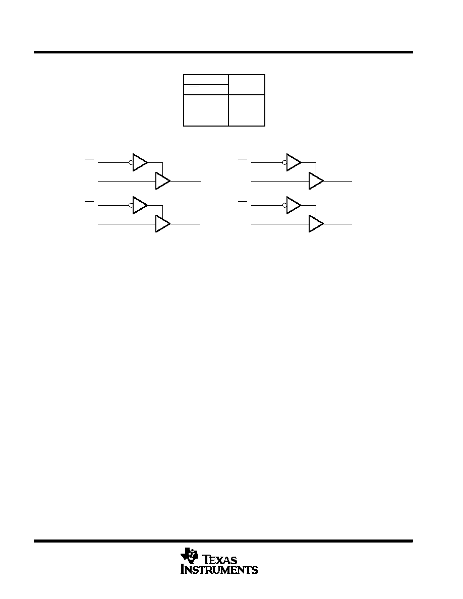
FUNCTION TABLE
(each buffer)
INPUTS
OUTPUT
OE
A
OUTPUT
Y
L
H
L
LL
H
X
Z
logic diagram (positive logic)
1
1OE
2
1A
1Y
3
4
2OE
5
2A
2Y
6
10
3OE
9
3A
3Y
8
13
4OE
12
4A
4Y
11
Pin numbers shown are for the D, DB, J, N, NS, PW, RGY, and W packages.
absolute maximum ratings over operating free-air temperature range (unless otherwise noted)
Supply voltage range, VCC
0.5 V to 7 V
. . . . . . . . . . . . . . . . . . . . . . . . . . . . . . . . . . . . . . . . . . . . . . . . . . . . . . . . . .
Input voltage range, VI (see Note 1)
0.5 V to 7 V
. . . . . . . . . . . . . . . . . . . . . . . . . . . . . . . . . . . . . . . . . . . . . . . . . .
Voltage range applied to any output in the high or power-off state, VO
0.5 V to 5.5 V
. . . . . . . . . . . . . . . . . . . .
Current into any output in the low state, IO: SN54ABT125
96 mA
. . . . . . . . . . . . . . . . . . . . . . . . . . . . . . . . . . . .
SN74ABT125
128 mA
. . . . . . . . . . . . . . . . . . . . . . . . . . . . . . . . . . .
Input clamp current, IIK (VI < 0)
18 mA
. . . . . . . . . . . . . . . . . . . . . . . . . . . . . . . . . . . . . . . . . . . . . . . . . . . . . . . . . . .
Output clamp current, IOK (VO < 0)
50 mA
. . . . . . . . . . . . . . . . . . . . . . . . . . . . . . . . . . . . . . . . . . . . . . . . . . . . . . . .
Package thermal impedance,
θJA (see Note 2): D package
86
°C/W
. . . . . . . . . . . . . . . . . . . . . . . . . . . . . . . . . . .
(see Note 2): DB package
96
°C/W
. . . . . . . . . . . . . . . . . . . . . . . . . . . . . . . . .
(see Note 2): N package
80
°C/W
. . . . . . . . . . . . . . . . . . . . . . . . . . . . . . . . . . .
(see Note 2): NS package
76
°C/W
. . . . . . . . . . . . . . . . . . . . . . . . . . . . . . . . .
(see Note 2): PW package
113
°C/W
. . . . . . . . . . . . . . . . . . . . . . . . . . . . . . . .
(see Note 3): RGY package
47
°C/W
. . . . . . . . . . . . . . . . . . . . . . . . . . . . . . . .
Storage temperature range, Tstg
65
°C to 150°C
. . . . . . . . . . . . . . . . . . . . . . . . . . . . . . . . . . . . . . . . . . . . . . . . . . .
Stresses beyond those listed under “absolute maximum ratings” may cause permanent damage to the device. These are stress ratings only, and
functional operation of the device at these or any other conditions beyond those indicated under “recommended operating conditions” is not
implied. Exposure to absolute-maximum-rated conditions for extended periods may affect device reliability.
NOTES:
1. The input and output negative-voltage ratings may be exceeded if the input and output clamp-current ratings are observed.
2. The package thermal impedance is calculated in accordance with JESD 51-7.
3. The package thermal impedance is calculated in accordance with JESD 51-5.
相關PDF資料 |
PDF描述 |
|---|---|
| SN74ABT125D | ABT SERIES, QUAD 1-BIT DRIVER, TRUE OUTPUT, PDSO14 |
| SN74ABT125PWR | ABT SERIES, QUAD 1-BIT DRIVER, TRUE OUTPUT, PDSO14 |
| SN74ABT126DBR | ABT SERIES, QUAD 1-BIT DRIVER, TRUE OUTPUT, PDSO14 |
| SN74ABT126NSRE4 | ABT SERIES, QUAD 1-BIT DRIVER, TRUE OUTPUT, PDSO14 |
| SN74ABT162244DGG | ABT SERIES, QUAD 4-BIT DRIVER, TRUE OUTPUT, PDSO48 |
相關代理商/技術參數 |
參數描述 |
|---|---|
| SN74ABT125N | 功能描述:緩沖器和線路驅動器 Tri-State Quad Bus RoHS:否 制造商:Micrel 輸入線路數量:1 輸出線路數量:2 極性:Non-Inverting 電源電壓-最大:+/- 5.5 V 電源電壓-最小:+/- 2.37 V 最大工作溫度:+ 85 C 安裝風格:SMD/SMT 封裝 / 箱體:MSOP-8 封裝:Reel |
| SN74ABT125N | 制造商:Texas Instruments 功能描述:Universal Bus Function IC |
| SN74ABT125NE4 | 功能描述:緩沖器和線路驅動器 Quad Bus Buff Gate With 3-State Outputs RoHS:否 制造商:Micrel 輸入線路數量:1 輸出線路數量:2 極性:Non-Inverting 電源電壓-最大:+/- 5.5 V 電源電壓-最小:+/- 2.37 V 最大工作溫度:+ 85 C 安裝風格:SMD/SMT 封裝 / 箱體:MSOP-8 封裝:Reel |
| SN74ABT125NS | 制造商:Rochester Electronics LLC 功能描述: 制造商:Texas Instruments 功能描述: |
| SN74ABT125NSR | 功能描述:緩沖器和線路驅動器 Quad Bus Buff Gate With 3-State Outputs RoHS:否 制造商:Micrel 輸入線路數量:1 輸出線路數量:2 極性:Non-Inverting 電源電壓-最大:+/- 5.5 V 電源電壓-最小:+/- 2.37 V 最大工作溫度:+ 85 C 安裝風格:SMD/SMT 封裝 / 箱體:MSOP-8 封裝:Reel |
發(fā)布緊急采購,3分鐘左右您將得到回復。