- 您現(xiàn)在的位置:買賣IC網(wǎng) > PDF目錄374848 > SN54AHC240J (Texas Instruments, Inc.) OCTAL BUFFERS/DRIVERS WITH 3-STATE OUTPUTS PDF資料下載
參數(shù)資料
| 型號(hào): | SN54AHC240J |
| 廠商: | Texas Instruments, Inc. |
| 英文描述: | OCTAL BUFFERS/DRIVERS WITH 3-STATE OUTPUTS |
| 中文描述: | 八路緩沖器/ 3司機(jī)態(tài)輸出 |
| 文件頁數(shù): | 1/18頁 |
| 文件大?。?/td> | 573K |
| 代理商: | SN54AHC240J |
SN54AHC240, SN74AHC240
OCTAL BUFFERS/DRIVERS
WITH 3-STATE OUTPUTS
SCLS251H – OCTOBER 1995 – REVISED JULY 2003
1
POST OFFICE BOX 655303
DALLAS, TEXAS 75265
Operating Range 2-V to 5.5-V V
CC
Latch-Up Performance Exceeds 250 mA
Per JESD 17
description/ordering information
These
specifically to improve the performance and
density of 3-state memory-address drivers, clock
drivers,
and
bus-oriented
transmitters.
octal
buffers/drivers
are
designed
receivers
and
The ’AHC240 devices are organized as two 4-bit
buffers/line drivers with separate output-enable
(OE) inputs. When OE is low, the device passes
data from the A inputs to the Y outputs. When OE
is high, the outputs are in the high-impedance
state.
To ensure the high-impedance state during power
up or power down, OE should be tied to V
CC
through a pullup resistor; the minimum value of
the resistor is determined by the current-sinking
capability of the driver.
ORDERING INFORMATION
TA
PACKAGE
ORDERABLE
PART NUMBER
TOP-SIDE
MARKING
PDIP – N
Tube
Tube
SN74AHC240N
SN74AHC240DW
SN74AHC240N
SOIC – DW
AHC240
Tape and reel
SN74AHC240DWR
–40
°
C to 85
°
C
SOP – NS
Tape and reel
SN74AHC240NSR
AHC240
SSOP – DB
Tape and reel
SN74AHC240DBR
HA240
TSSOP – PW
Tube
SN74AHC240PW
HA240
Tape and reel
SN74AHC240PWR
TVSOP – DGV
Tape and reel
SN74AHC240DGVR
HA240
CDIP – J
Tube
SNJ54AHC240J
SNJ54AHC240J
–55
°
C to 125
°
C
CFP – W
Tube
SNJ54AHC240W
SNJ54AHC240W
LCCC – FK
Tube
SNJ54AHC240FK
SNJ54AHC240FK
Package drawings, standard packing quantities, thermal data, symbolization, and PCB design guidelines
are available at www.ti.com/sc/package.
Copyright
2003, Texas Instruments Incorporated
On products compliant to MIL-PRF-38535, all parameters are tested
unless otherwise noted. On all other products, production
processing does not necessarily include testing of all parameters.
PRODUCTION DATA information is current as of publication date.
Products conform to specifications per the terms of Texas Instruments
standard warranty. Production processing does not necessarily include
testing of all parameters.
Please be aware that an important notice concerning availability, standard warranty, and use in critical applications of
Texas Instruments semiconductor products and disclaimers thereto appears at the end of this data sheet.
1
2
3
4
5
6
7
8
9
10
20
19
18
17
16
15
14
13
12
11
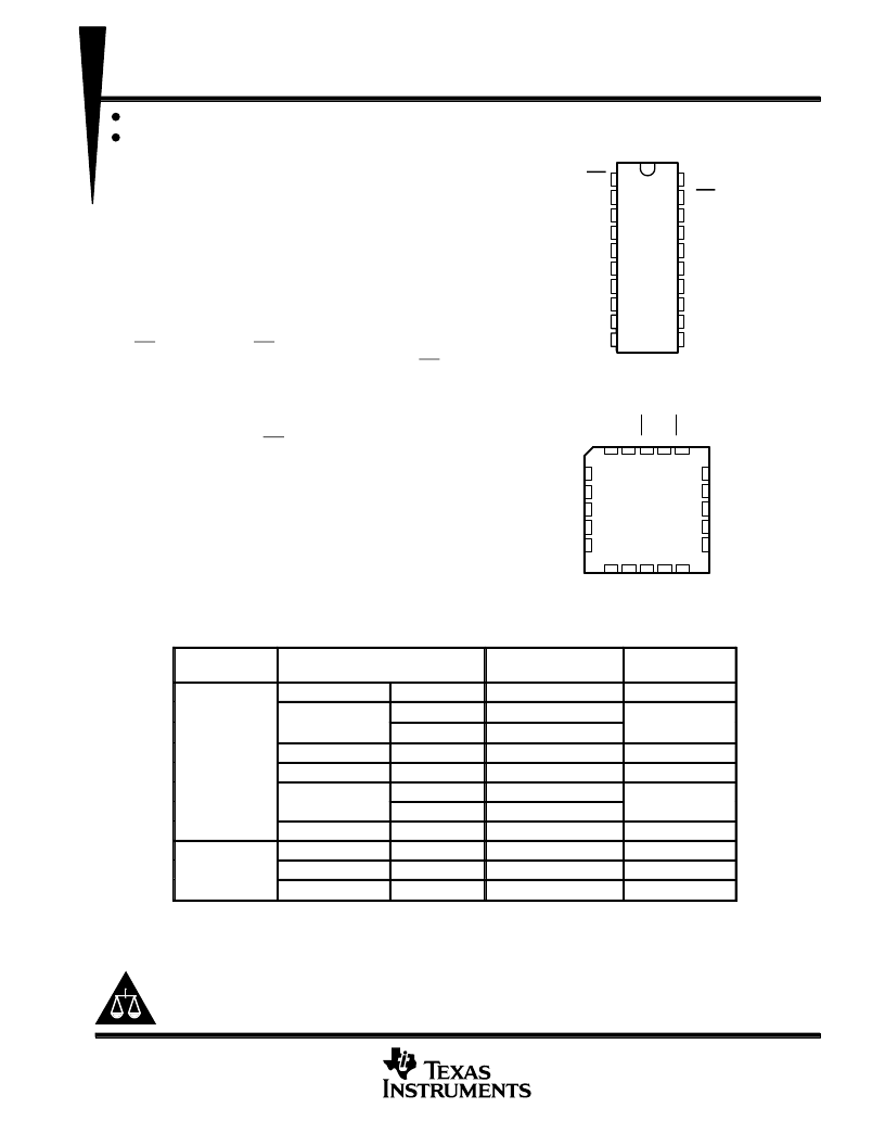
1OE
1A1
2Y4
1A2
2Y3
1A3
2Y2
1A4
2Y1
GND
V
CC
2OE
1Y1
2A4
1Y2
2A3
1Y3
2A2
1Y4
2A1
SN54AHC240 . . . J OR W PACKAGE
SN74AHC240 . . . DB, DGV, DW, N, NS, OR PW PACKAGE
(TOP VIEW)
3
2
1 20 19
9 10 11 12 13
4
5
6
7
8
18
17
16
15
14
1Y1
2A4
1Y2
2A3
1Y3
1A2
2Y3
1A3
2Y2
1A4
SN54AHC240 . . . FK PACKAGE
(TOP VIEW)
2
1
1
1
2
2
2
G
2
V
C
相關(guān)PDF資料 |
PDF描述 |
|---|---|
| SN54AHC240W | OCTAL BUFFERS/DRIVERS WITH 3-STATE OUTPUTS |
| SN54AHCT00FK | QUADRUPLE 2-INPUT POSITIVE-NAND GATES |
| SN54AHCT00J | QUADRUPLE 2-INPUT POSITIVE-NAND GATES |
| SN54AHCT00W | QUADRUPLE 2-INPUT POSITIVE-NAND GATES |
| SN74AHCT00DB | QUADRUPLE 2-INPUT POSITIVE-NAND GATES |
相關(guān)代理商/技術(shù)參數(shù) |
參數(shù)描述 |
|---|---|
| SN54AHC240W | 制造商:TI 制造商全稱:Texas Instruments 功能描述:OCTAL BUFFERS/DRIVERS WITH 3-STATE OUTPUTS |
| SN54AHC244 | 制造商:TI 制造商全稱:Texas Instruments 功能描述:OCTAL BUFFERS/DRIVERS WITH 3-STATE OUTPUTS |
| SN54AHC244_07 | 制造商:TI 制造商全稱:Texas Instruments 功能描述:OCTAL BUFFERS/DRIVERS WITH 3-STATE OUTPUTS |
| SN54AHC244_08 | 制造商:TI 制造商全稱:Texas Instruments 功能描述:OCTAL BUFFERS/DRIVERS WITH 3-STATE OUTPUTS |
| SN54AHC244FK | 制造商:TI 制造商全稱:Texas Instruments 功能描述:OCTAL BUFFERS/DRIVERS WITH 3-STATE OUTPUTS |
發(fā)布緊急采購,3分鐘左右您將得到回復(fù)。