- 您現(xiàn)在的位置:買賣IC網(wǎng) > PDF目錄8718 > SL23EP05SC-1 (Silicon Laboratories Inc)IC BUFFER 220MHZ 5CH 3.3V 8SOIC PDF資料下載
參數(shù)資料
| 型號(hào): | SL23EP05SC-1 |
| 廠商: | Silicon Laboratories Inc |
| 文件頁數(shù): | 5/11頁 |
| 文件大?。?/td> | 0K |
| 描述: | IC BUFFER 220MHZ 5CH 3.3V 8SOIC |
| 標(biāo)準(zhǔn)包裝: | 100 |
| 系列: | EProClock® |
| 類型: | * |
| PLL: | 是 |
| 輸入: | 時(shí)鐘 |
| 輸出: | 時(shí)鐘 |
| 電路數(shù): | 1 |
| 比率 - 輸入:輸出: | 1:5 |
| 差分 - 輸入:輸出: | 無/無 |
| 頻率 - 最大: | 220MHz |
| 除法器/乘法器: | 是/是 |
| 電源電壓: | 2.3 V ~ 3.6 V |
| 工作溫度: | 0°C ~ 70°C |
| 安裝類型: | * |
| 封裝/外殼: | * |
| 供應(yīng)商設(shè)備封裝: | * |
| 包裝: | * |
Rev 0.0, September 18, 2006
Page 3 of 11
SL23EP05
General Description
The SL23EP09 is a low skew, low jitter Zero Delay Buffer with
very low operating current.
The product includes an on-chip high performance PLL that
locks into the input reference clock and produces nine (9)
output clock drivers tracking the input reference clock for
systems requiring clock distribution.
in addition to CLKOUT that is used for internal PLL feedback,
there are two (2) banks with four (4) outputs in each bank,
bringing the number of total available output clocks to nine (9).
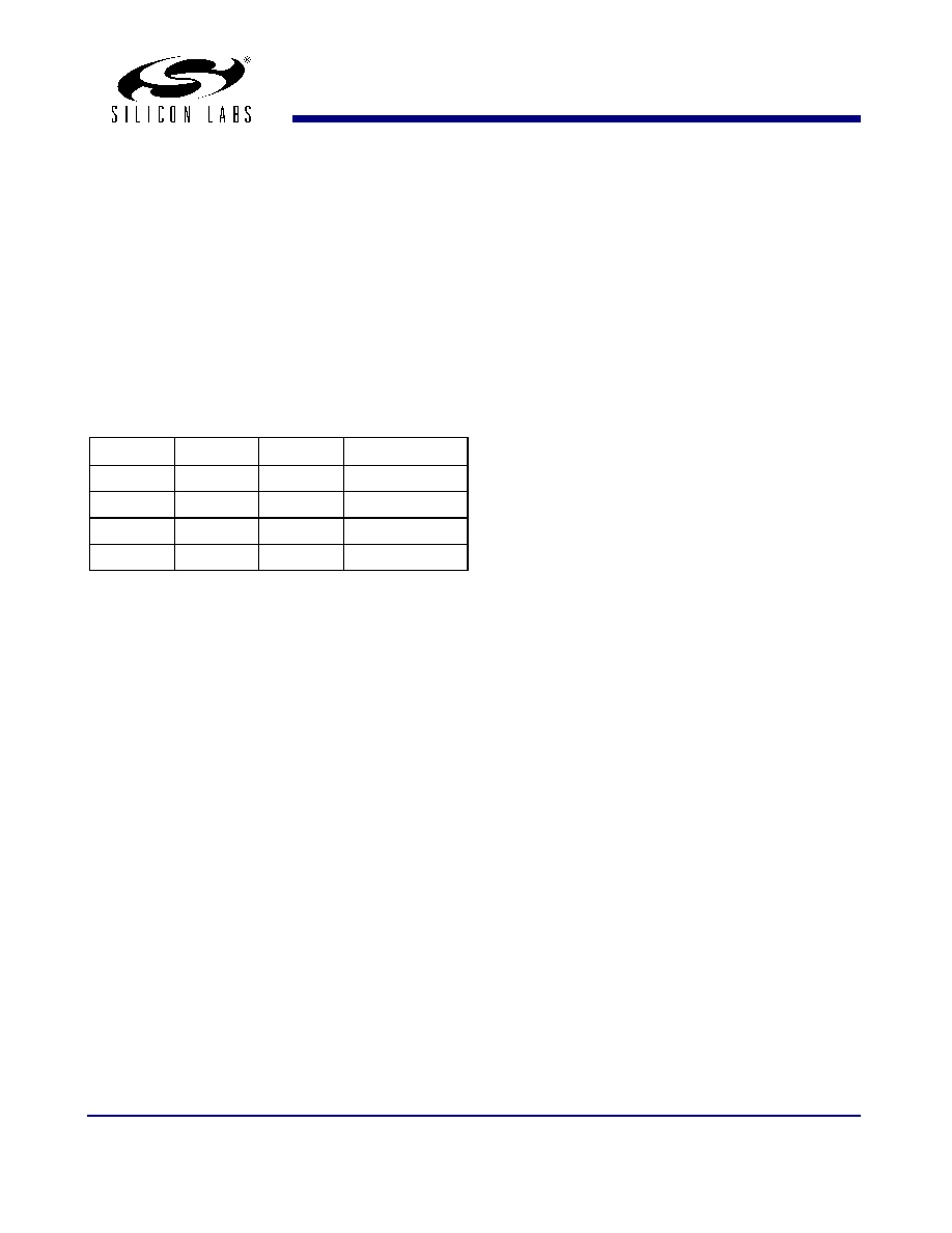
Input and output Frequency Range
The input and output frequency range is the same. But, it
depends on VDD and drive levels as given in the below
Table 1.
VDD(V)
Drive
Min(MHz)
Max(MHz)
3.3
HIGH
10
220
3.3
STD
10
167
2.5
HIGH
10
200
2.5
STD
10
133
Table 1. Input/Output Frequency Range
If the input clock frequency is less than 2 MHz or floating, this
is detected by an input frequency detection circuitry and all
nine (9) clock outputs are forced to Hi-Z. The PLL is shutdown
to save power. In this shutdown state, the product draws less
than 25 μA supply current.
SpreadThru
Feature
If a Spread Spectrum Clock (SSC) were to be used as an
input clock, the SL23EP09 is designed to pass the modulated
Spread Spectrum Clock (SSC) signal from its reference input
to the output clocks. The same spread characteristics at the
input are passed through the PLL and drivers without any
degradation in spread percent (%), spread profile and
modulation frequency.
Select Input Control
The SL23EP09 provides two (2) input select control pins
called S1 and S2. This feature enables users to selects
various states of output clock banks-A and bank-B, output
source and PLL shutdown features as shown in the Table 2.
The S1 (Pin-9) and S2 (Pin-
8) inputs include 150 kΩ weak
pull-down resistors to GND.
PLL Bypass Mode
If the S1 and S2 pins are logic Low(0) and High(1)
respectively, the on-chip PLL is shutdown and bypassed, and
all the nine output clocks bank
A, bank B and CLKOUT
clocks are driven by directly from the reference input clock. In
this operation mode SL23EP09 works like a non-ZDB product.
High and Low-Drive Product Options
The SL23EP09 is offered with High-Drive “-1H” and Standard-
Drive “-1” options. These drive options enable the users to
control load levels, frequency range and EMI control. Refer to
the AC electrical tables for the details.
Skew and Zero Delay
All outputs should drive the similar load to achieve output-to-
output skew and input-to-output specifications given in the AC
electrical tables. However, Zero delay between input and
outputs can be adjusted by changing the loading of CLKOUT
relative to the banks A and B clocks since CLKOUT is the
feedback to the PLL.
Power Supply Range (VDD)
The SL23EP09 is designed to operate in a wide power supply
range from 2.250V (Min) to 3.360V (Max). This power supply
range complies with 3.3V+/-10% and 2.5V+/-10% standard
power supply requirements used in most systems. An internal
on-chip voltage regulator is used to supply PLL constant
power supply of 1.8V, leading to a consistent and stable PLL
electrical performance in terms of skew, jitter and power
dissipation. Contact SLI for 1.8V power supply version ZDB
called SL23EPL09.
相關(guān)PDF資料 |
PDF描述 |
|---|---|
| V24A36H400BG | CONVERTER MOD DC/DC 36V 400W |
| SL2309ZI-1 | IC BUFFER 140MHZ 9CH3.3V 16TSSOP |
| SL2309SI-1H | IC BUFFER 140MHZ 9CH 3.3V 16SOIC |
| V24A36H400BF3 | CONVERTER MOD DC/DC 36V 400W |
| VI-J5B-MZ-F4 | CONVERTER MOD DC/DC 95V 25W |
相關(guān)代理商/技術(shù)參數(shù) |
參數(shù)描述 |
|---|---|
| SL23EP05SC-1H | 功能描述:時(shí)鐘緩沖器 10-220MHz 5 Outputs ZDB 3.3-2.5V Hi Drv RoHS:否 制造商:Texas Instruments 輸出端數(shù)量:5 最大輸入頻率:40 MHz 傳播延遲(最大值): 電源電壓-最大:3.45 V 電源電壓-最小:2.375 V 最大功率耗散: 最大工作溫度:+ 85 C 最小工作溫度:- 40 C 封裝 / 箱體:LLP-24 封裝:Reel |
| SL23EP05SC-1HT | 功能描述:時(shí)鐘緩沖器 10-220MHz 5 Outputs ZDB 3.3-2.5V Hi Drv RoHS:否 制造商:Texas Instruments 輸出端數(shù)量:5 最大輸入頻率:40 MHz 傳播延遲(最大值): 電源電壓-最大:3.45 V 電源電壓-最小:2.375 V 最大功率耗散: 最大工作溫度:+ 85 C 最小工作溫度:- 40 C 封裝 / 箱體:LLP-24 封裝:Reel |
| SL23EP05SC-1T | 功能描述:時(shí)鐘緩沖器 10-220MHz 5 Outputs ZDB 3.3-2.5V RoHS:否 制造商:Texas Instruments 輸出端數(shù)量:5 最大輸入頻率:40 MHz 傳播延遲(最大值): 電源電壓-最大:3.45 V 電源電壓-最小:2.375 V 最大功率耗散: 最大工作溫度:+ 85 C 最小工作溫度:- 40 C 封裝 / 箱體:LLP-24 封裝:Reel |
| SL23EP05SI-1 | 功能描述:時(shí)鐘緩沖器 10-220MHz 5 Outputs ZDB 3.3-2.5V RoHS:否 制造商:Texas Instruments 輸出端數(shù)量:5 最大輸入頻率:40 MHz 傳播延遲(最大值): 電源電壓-最大:3.45 V 電源電壓-最小:2.375 V 最大功率耗散: 最大工作溫度:+ 85 C 最小工作溫度:- 40 C 封裝 / 箱體:LLP-24 封裝:Reel |
| SL23EP05SI-1H | 功能描述:時(shí)鐘緩沖器 10-220MHz 5 Outputs ZDB 3.3-2.5V Hi Drv RoHS:否 制造商:Texas Instruments 輸出端數(shù)量:5 最大輸入頻率:40 MHz 傳播延遲(最大值): 電源電壓-最大:3.45 V 電源電壓-最小:2.375 V 最大功率耗散: 最大工作溫度:+ 85 C 最小工作溫度:- 40 C 封裝 / 箱體:LLP-24 封裝:Reel |
發(fā)布緊急采購,3分鐘左右您將得到回復(fù)。