- 您現(xiàn)在的位置:買賣IC網(wǎng) > PDF目錄358395 > SK18-TP (MICRO COMMERCIAL COMPONENTS) RECT SCHOTTKY 1A 80V DO-214AA PDF資料下載
參數(shù)資料
| 型號(hào): | SK18-TP |
| 廠商: | MICRO COMMERCIAL COMPONENTS |
| 元件分類: | 參考電壓二極管 |
| 英文描述: | RECT SCHOTTKY 1A 80V DO-214AA |
| 中文描述: | 1 A, 80 V, SILICON, SIGNAL DIODE, DO-214AA |
| 封裝: | ROHS COMPLIANT, PLASTIC, HSMB, 2 PIN |
| 文件頁數(shù): | 1/4頁 |
| 文件大小: | 239K |
| 代理商: | SK18-TP |
SK12
THRU
SK110
1 Amp Schottky
Rectifier
20 to 100 Volts
Features
Lead Free Finish/Rohs Compliant (Note1) ("P"Suffix designates
Compliant. See ordering information)
Low Forward Voltage
Guard Ring Protection
High Current Capability
Low Thermal Resistance
Epoxy meets UL 94 V-0 flammability rating
Moisture Sensitivity Level 1
Operating Temperature
(Tj)
: -55
°
C to +125
°
C
Storage Temperature
(Tstg)
: -55
°
C to +150
°
C
Maximum Thermal Resistance; 28
°
C/W Junction To Lead
MCC
Catalog
Number
Device
Marking
Maximum
Recurrent
Peak Reverse
Voltage
20V
30V
40V
50V
60V
80V
100V
Maximum
RMS
Voltage
Maximum
DC
Blocking
Voltage
20V
30V
40V
50V
60V
80V
100V
SK12
SK13
SK14 SK14
SK15
SK16
SK18
SK110
Electrical Characteristics @ 25
°
C Unless Otherwise Specified
Average Forward
Current
Peak Forward Surge
Current
Maximum
Instantaneous
Forward Voltage
SK12
SK13
SK14
SK15-16
SK18-110
Maximum DC Reverse
Current At Rated DC
Blocking Voltage
Typical Junction
Capacitance
SK12
SK13-SK110
*Pulse test: Pulse width 300
μ
sec, Duty cycle 2%
Note: 1.
High Temperature Solder Exemptions Applied, see EU Directive Annex 7.
SK12
SK13
14V
21V
28V
35V
42V
56V
70V
SK15
SK16
SK18
SK110
I
F(AV)
1.0A
T
J
= 90
°
C
I
FSM
30A
8.3ms, half sine
V
F
.45V
.55V
.60V
.72V
.85V
I
FM
= 1.0A;
T
a
= 25
°
C*
C
J
11
0pF
3
0pF
Measured at
1.0MHz, V
R
=4.0V
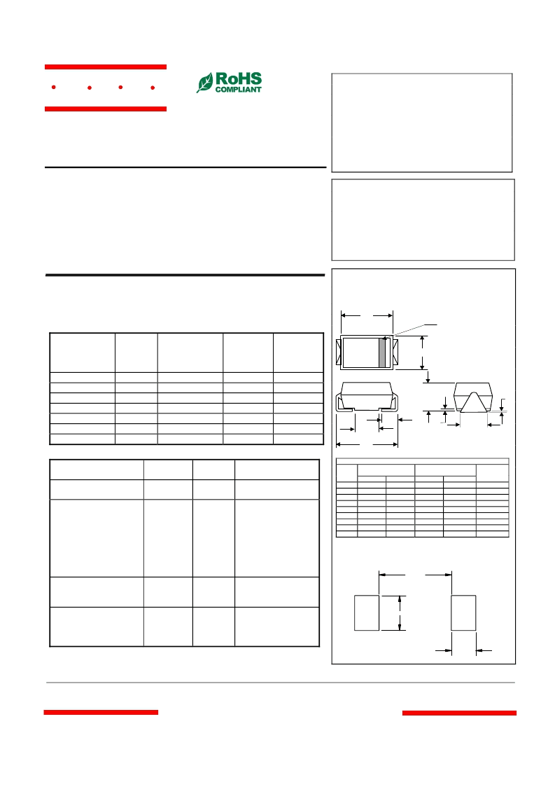
DO-214A
A
(
H
SMB) (
Round Lead
)
H
J
E
F
G
A
B
D
C
Cathode Band
0.070”
0.090"
0.085”
SUGGESTED SOLDER
PAD LAYOUT
DIMENSIONS
INCHES
MIN
.078
.075
.002
MM
DIM
A
B
C
D ----- .02
E
.035
F
.065
G
.205
H
.160
J
.130
MAX
.116
.089
.008
MIN
1.98
1.90
.05
----- .51
.90
1.65
5.21
4.06
3.30
MAX
2.95
2.25
.20
NOTE
.055
.091
.224
.180
.155
1.40
2.32
5.69
4.57
3.94
omp
onents
20736 Marilla Street Chatsworth
M C C
Revision:
A
20
11
/0
1
/
01
I
R
0.5mA
20mA
T
A
= 25
°
C
T
A
= 100
°
C
TM
Micro Commercial Components
Maximum Ratings
www.
mc c semi
.c om
相關(guān)PDF資料 |
PDF描述 |
|---|---|
| SK210-TP | DIODE SCHOTTKY 2A 100V SMB |
| SK22-TP | DIODE SCHOTTKY 2A 20V SMB |
| SK23-TP | DIODE SCHOTTKY 2A 30V SMB |
| SK24-TP | DIODE SCHOTTKY 2A 40V SMB |
| SK25-TP | DIODE SCHOTTKY 2A 50V SMB |
相關(guān)代理商/技術(shù)參數(shù) |
參數(shù)描述 |
|---|---|
| SK18-TP (SMBSR108) | 制造商:Micro Commercial Components (MCC) 功能描述:DIODE SCHOTTKY 80V 1A DO214AA |
| SK18V | 制造商:RCA 功能描述: |
| SK19 | 制造商:SYNSEMI 制造商全稱:SYNSEMI 功能描述:SURFACE MOUNT SCHOTTKY BARRIER RECTIFIERS |
| SK-19/37 | 制造商:Fischer Elektronik GmbH & Co KG 功能描述: |
| SK1900 | 制造商:SEMTECH 制造商全稱:Semtech Corporation 功能描述:1:9 Signal Distribution |
發(fā)布緊急采購,3分鐘左右您將得到回復(fù)。