- 您現在的位置:買賣IC網 > PDF目錄21894 > SI4123-EVB (Silicon Laboratories Inc)BOARD EVALUATION FOR SI4123 PDF資料下載
參數資料
| 型號: | SI4123-EVB |
| 廠商: | Silicon Laboratories Inc |
| 文件頁數: | 33/36頁 |
| 文件大小: | 0K |
| 描述: | BOARD EVALUATION FOR SI4123 |
| 標準包裝: | 1 |
| 類型: | 合成器 |
| 適用于相關產品: | SI4123 |
| 所含物品: | 板和光盤 |
第1頁第2頁第3頁第4頁第5頁第6頁第7頁第8頁第9頁第10頁第11頁第12頁第13頁第14頁第15頁第16頁第17頁第18頁第19頁第20頁第21頁第22頁第23頁第24頁第25頁第26頁第27頁第28頁第29頁第30頁第31頁第32頁當前第33頁第34頁第35頁第36頁
Si4133
6
Rev. 1.61
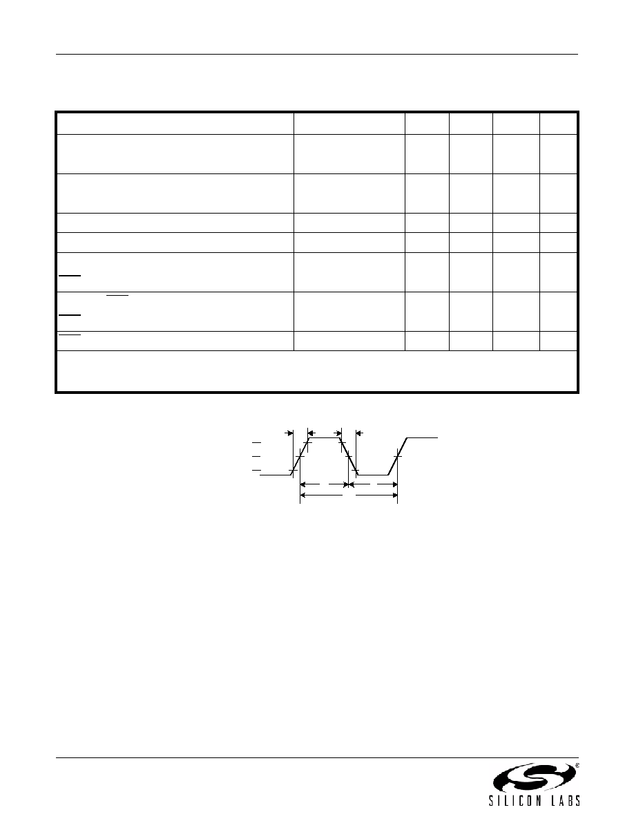
Figure 1. SCLK Timing Diagram
Table 4. Serial Interface Timing
(V
DD = 2.7 to 3.6 V, TA = –40 to 85 °C)
Parameter1
Symbol
Test Condition
Min
Typ
Max
Unit
SCLK Cycle Time
tclk
40
—
ns
SCLK Rise Time
tr
—
50
ns
SCLK Fall Time
t
f
—
50
ns
SCLK High Time
th
10
—
ns
SCLK Low Time
tl
10
—
ns
SDATA Setup Time to SCLK
2
t
su
5
—
ns
SDATA Hold Time from SCLK
2
thold
0
—
ns
SEN
to SCLKDelay Time2
ten1
10
—
ns
SCLK
to SENDelay Time2
t
en2
12
—
ns
SEN
to SCLKDelay Time2
ten3
12
—
ns
SEN Pulse Width
tw
10
—
ns
Notes:
1. All timing is referenced to the 50% level of the waveforms unless otherwise noted.
2. Timing is not referenced to 50% level of the waveform. See Figure 2.
SCLK
80%
20%
50%
t
r
t
f
t
l
t
clk
t
h
相關PDF資料 |
PDF描述 |
|---|---|
| ZMN2400DK | KIT DEV ZIGBEE MOD ZMN2400 1MW |
| CME8000-DB | BOARD DEMO FOR CME8000 |
| SI4122-EVB | BOARD EVALUATION FOR SI4122 |
| PSL0101WBFC1 | LED WHITE 75LM 350MA 3000K SSML |
| PSL0101WBFA1 | LED WHITE 100LM 350MA 3000K SSML |
相關代理商/技術參數 |
參數描述 |
|---|---|
| SI4123G | 制造商:SILABS 制造商全稱:SILABS 功能描述:DUAL-BAND RF SYNTHESIZER WITH INTEGRATED VCOS FOR GSM AND GPRS WIRELESS COMMUNICATIONS |
| SI4123G-BM | 制造商:Silicon Laboratories Inc 功能描述: |
| SI4123G-BMR | 功能描述:鎖相環(huán) - PLL CONTACT SILICON LABS FOR AVAILABILITY RoHS:否 制造商:Silicon Labs 類型:PLL Clock Multiplier 電路數量:1 最大輸入頻率:710 MHz 最小輸入頻率:0.002 MHz 輸出頻率范圍:0.002 MHz to 808 MHz 電源電壓-最大:3.63 V 電源電壓-最小:1.71 V 最大工作溫度:+ 85 C 最小工作溫度:- 40 C 封裝 / 箱體:QFN-36 封裝:Tray |
| SI4123G-BT | 制造商:SILABS 制造商全稱:SILABS 功能描述:DUAL-BAND RF SYNTHESIZER WITH INTEGRATED VCOS FOR GSM AND GPRS WIRELESS COMMUNICATIONS |
發(fā)布緊急采購,3分鐘左右您將得到回復。