- 您現(xiàn)在的位置:買賣IC網(wǎng) > PDF目錄26874 > SFH628A-4 (VISHAY SEMICONDUCTORS) 1 CHANNEL AC INPUT-TRANSISTOR OUTPUT OPTOCOUPLER PDF資料下載
參數(shù)資料
www.vishay.com
For technical questions, contact: optocoupleranswers@vishay.com
Document Number: 83722
2
Rev. 1.9, 24-Mar-11
This datasheet is subject to change without notice.
THE PRODUCT DESCRIBED HEREIN AND THIS DATASHEET ARE SUBJECT TO SPECIFIC DISCLAIMERS, SET FORTH AT www.vishay.com/doc?91000
SFH628A, SFH6286
Vishay Semiconductors Optocoupler, Phototransistor Output,
AC Input, Low Input Current
Notes
Stresses in excess of the absolute maximum ratings can cause permanent damage to the device. Functional operation of the device is not
implied at these or any other conditions in excess of those given in the operational sections of this document. Exposure to absolute
maximum ratings for extended periods of the time can adversely affect reliability.
(
1) Refer to reflow profile for soldering conditions for surface mounted devices (SMD). Refer to wave profile for soldering conditions for through
hole devices (DIP).
Note
Minimum and maximum values are testing requirements. Typical values are characteristics of the device and are the result of engineering
evaluation. Typical values are for information only and are not part of the testing requirements.
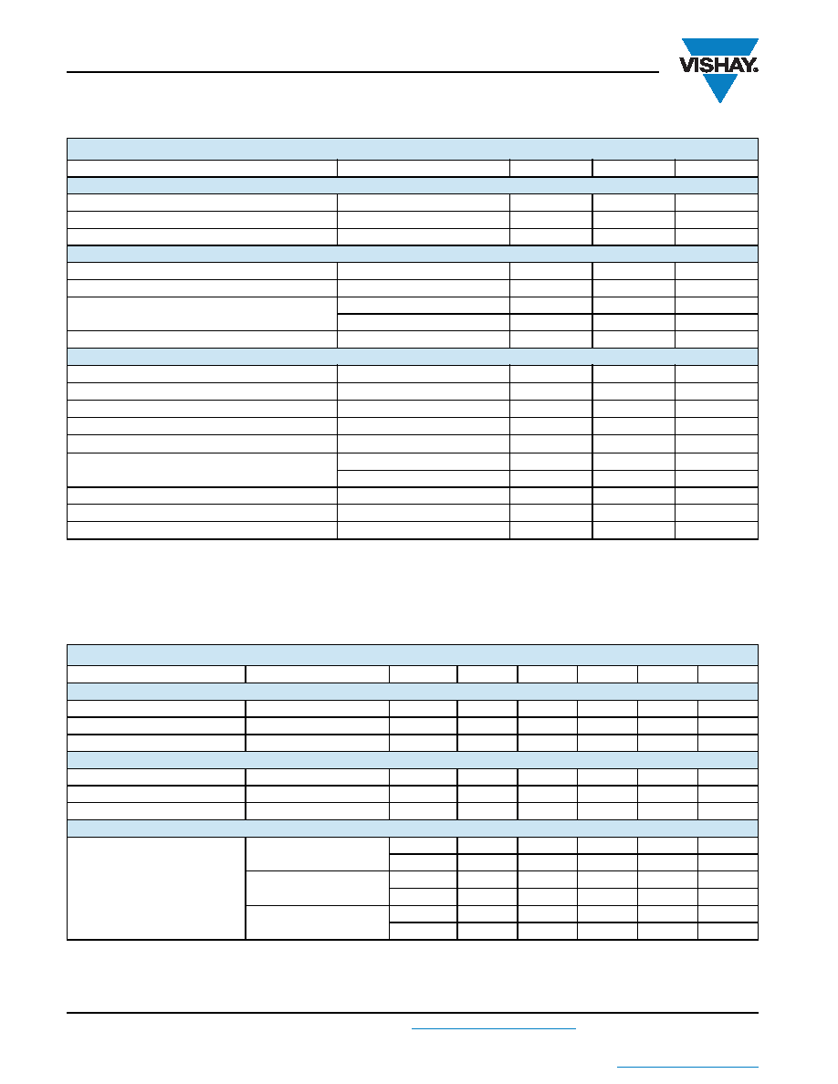
ABSOLUTE MAXIMUM RATINGS (Tamb = 25 °C, unless otherwise specified)
PARAMETER
TEST CONDITION
SYMBOL
VALUE
UNIT
INPUT
DC forward current
IF
± 50
mA
Surge forward current
t
10 μs
IFSM
± 2.5
A
Power dissipation
Pdiss
76
mW
OUTPUT
Collector emitter voltage
VCE
55
V
Emitter collector voltage
VEC
7V
Collector current
IC
50
mA
tp 1 ms
IC
100
mA
Power dissipation
Pdiss
150
mW
COUPLER
Isolation test voltage
VISO
5300
VRMS
Creepage distance
7mm
Clearance distance
7mm
Insulation thickness between
0.4
mm
Comparative tracking index per DIN IEC112/
175
Isolation resistance
VIO = 500 V, Tamb = 25 °C
RIO
1012
VIO = 500 V, Tamb = 100 °C
RIO
1011
Storage temperature range
Tstg
- 55 to + 150
°C
Ambient temperature range
Tamb
- 55 to +100
°C
Soldering temperature (1)
max. 10 s, dip soldering distance
Tsld
260
°C
ELECTRICAL CHARACTERISTICS (Tamb = 25 °C, unless otherwise specified)
PARAMETER
TEST CONDITION
PART
SYMBOL
MIN.
TYP.
MAX.
UNIT
INPUT
Forward voltage
IF = ± 5 mA
VF
1.1
1.5
V
Capacitance
VR = 0 V, f = 1 MHz
CO
45
pF
Thermal resistance
Rthja
1070
K/W
OUTPUT
Collector emitter leakage current
VCE = 10 V
ICEO
10
200
nA
Collector emitter capacitance
VCE = 5 V, f = 1 MHz
CCE
7pF
Thermal resistance
Rthja
500
K/W
COUPLER
Collector emitter saturation
voltage
IF = ± 1 mA, IC = 0.5 mA
SFH628A-2
VCEsat
0.25
0.4
V
SFH6286-2
VCEsat
0.25
0.4
V
IF = ± 1 mA, IC = 0.8 mA
SFH628A-3
VCEsat
0.25
0.4
V
SFH6286-3
VCEsat
0.25
0.4
V
IF = ± 1 mA, IC = 1.25 mA
SFH628A-4
VCEsat
0.25
0.4
V
SFH6286-4
VCEsat
0.25
0.4
V
相關(guān)PDF資料 |
PDF描述 |
|---|---|
| SFH6286-4X001 | 1 CHANNEL AC INPUT-TRANSISTOR OUTPUT OPTOCOUPLER |
| SFH6286-4-X001 | 1 CHANNEL AC INPUT-TRANSISTOR OUTPUT OPTOCOUPLER |
| SFH628A-4-X001 | 1 CHANNEL AC INPUT-TRANSISTOR OUTPUT OPTOCOUPLER |
| SFH628A-2-X016 | 1 CHANNEL AC INPUT-TRANSISTOR OUTPUT OPTOCOUPLER |
| SFH628A-2-X016 | 1 CHANNEL AC INPUT-TRANSISTOR OUTPUT OPTOCOUPLER |
相關(guān)代理商/技術(shù)參數(shù) |
參數(shù)描述 |
|---|---|
| SFH628A-4 | 制造商:Vishay Semiconductors 功能描述:Optocoupler |
| SFH628A-4-X006 | 制造商:VISHAY 制造商全稱:Vishay Siliconix 功能描述:Optocoupler, Phototransistor Output, AC Input, Low Input Current |
| SFH628A-4X016 | 功能描述:晶體管輸出光電耦合器 Phototransistor Out AC-In CTR>160-500% RoHS:否 制造商:Vishay Semiconductors 輸入類型:DC 最大集電極/發(fā)射極電壓:70 V 最大集電極/發(fā)射極飽和電壓:0.4 V 絕緣電壓:5300 Vrms 電流傳遞比:100 % to 200 % 最大正向二極管電壓:1.65 V 最大輸入二極管電流:60 mA 最大集電極電流:100 mA 最大功率耗散:100 mW 最大工作溫度:+ 110 C 最小工作溫度:- 55 C 封裝 / 箱體:DIP-4 封裝:Bulk |
| SFH6315 | 制造商:INFINEON 制造商全稱:Infineon Technologies AG 功能描述:HIGH SPEED OPTOCOUPLER |
| SFH6315T | 功能描述:高速光耦合器 1Mbd Open Collector Single Channel RoHS:否 制造商:Avago Technologies 電流傳遞比: 最大波特率: 最大正向二極管電壓:1.75 V 最大反向二極管電壓:5 V 最大功率耗散:40 mW 最大工作溫度:+125 C 最小工作溫度:- 40 C 封裝 / 箱體:SOIC-5 封裝:Tube |
發(fā)布緊急采購,3分鐘左右您將得到回復(fù)。