- 您現(xiàn)在的位置:買(mǎi)賣(mài)IC網(wǎng) > PDF目錄385840 > SF1174B (RF Monolithics, Inc.) 374.00 MHz SAW Filter PDF資料下載
參數(shù)資料
| 型號(hào): | SF1174B |
| 廠(chǎng)商: | RF Monolithics, Inc. |
| 英文描述: | 374.00 MHz SAW Filter |
| 中文描述: | 374.00兆赫SAW濾波器 |
| 文件頁(yè)數(shù): | 1/3頁(yè) |
| 文件大小: | 107K |
| 代理商: | SF1174B |
RF Monolithics, Inc.
RFM Europe
1999 by RF Monolithics, Inc. The stylized RFM logo are registered trademarks of RF Monolithics, Inc.
Phone: (972) 233-2903
Phone: 44 1963 251383
Fax: (972) 387-8148
Fax: 44 1963 251510
E-mail: info@rfm.com
http://www.rfm.com
SF1174B 532-1174-001 121604 RevA
Page 1 of 3
Electrical Characteristics
Characteristic
Sym
f
C
IL
BW
3
Notes
1
Min
Typ
Max
Units
MHz
dB
MHz
dB
P-P
ns
P-P
Nominal Center Frequency
Passband
374.000
Insertion Loss at fc
3 dB Passband
8.7
23
10.0
1, 2
17
Amplitude Ripple over fc ±7.0 MHz
Group Delay Variation over fc ±7.0
fc -100 to fc -33 MHz
fc -33 to fc -22 MHz
fc -22 to fc -16.5 MHz
fc +16.5 to fc +22 MHz
fc +22 to fc +43 MHz
fc +43 to fc +100 MHz
0.8
61
54
53
40
44
48
49
1.0
100
GDV
Rejection
1, 2, 3
45
40
30
30
35
40
dB
Operating Temperature Range
T
A
1
-10
+85
°C
Differential Input / Output Impedance Match
Case Style
Lid Symbolization (YY=year, WW=week, S=shift)
External L-C
SM5050-8 5 X 5 mm Nominal Footprint
447, YYWWS
SM5050-8
Designed for WLAN IF Applications
Low Insertion Loss
5.0 x 5.0 x 1.7 mm Suface-Mount Case
Differential or Single Ended Input and Output
Complies with Directive 2002/95/EC (RoHS)
Absolute Maximum Ratings
Rating
Value
+10
30
-40 to +85
Units
dBm
VDC
°C
Maximum Incident Power in Passband
Max. DC voltage between any 2 terminals
Storage Temperature Range
Suitable for lead-free soldering - Max Soldering Profile
260°C for 30 s
374.00 MHz
SAW Filter
SF1174B
Connection
Port 1 Hot
Port 1 Gnd Return
Port 2 Hot
Port 2 Gnd Return
Case Ground
Terminals
2
3
6
7
All others
Electrical Connections
1.
Unless noted otherwise, all specifications apply over the operating temperature
range with filter soldered to the specified demonstration board with impedance
matching to 50
and measured with 50
network analyzer.
Unless noted otherwise, all frequency specifications are referenced to the nom-
inal center frequency, fc.
Rejection is measured as attenuation below the minimum IL point in the pass-
band. Rejection in final user application is dependent on PCB layout and exter-
nal impedance matching design. See Application Note No. 42 for details.
"LRIP" or "L" after the part number indicates "low rate initial production" and
"ENG" or "E" indicates "engineering prototypes."
2.
3.
4.
5.
The design, manufacturing process, and specifications of this filter are subject
to change.
Either Port 1 or Port 2 may be used for either input or output in the design.
However, impedances and impedance matching may vary between Port 1 and
Port 2, so that the filter must always be installed in one direction per the circuit
design.
US and international patents may apply.
RFM, stylized RFM logo, and RF Monolithics, Inc. are registered trademarks of
RF Monolithics, Inc.
Copyright 1999, RF Monolithics Inc.
Electrostatic Sensitive Device. Observe precautions for handling.
6.
7.
8.
9.
10.
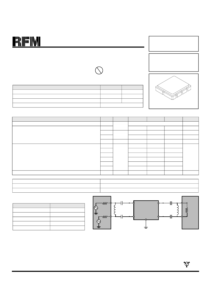
27nH
27nH
100
100
RF IC
SAW Filter
TOP VIEW
RF IC
12pf
12pf
200
12pf
12pf
pin 2
pin 3
pin 7
pin 6
figure 1
Notes:
Pb
相關(guān)PDF資料 |
PDF描述 |
|---|---|
| SF1174D | 374.00 MHz SAW Filter |
| SF1177A | 57.6 MHz SAW Filter |
| SF1179B | 184.14 MHz SAW Filter |
| SF1186B-2 | 1575.42 MHz SAW Filter |
| SF1188C | 465.00 MHz SAW Filter |
相關(guān)代理商/技術(shù)參數(shù) |
參數(shù)描述 |
|---|---|
| SF1174D | 功能描述:信號(hào)調(diào)節(jié) 374.0MHz, WLAN IF SAW Filter RoHS:否 制造商:EPCOS 產(chǎn)品:Duplexers 頻率:782 MHz, 751 MHz 頻率范圍: 電壓額定值: 帶寬: 阻抗:50 Ohms 端接類(lèi)型:SMD/SMT 封裝 / 箱體:2.5 mm x 2 mm 工作溫度范圍:- 30 C to + 85 C 封裝:Reel |
| SF1177A | 功能描述:信號(hào)調(diào)節(jié) 57.6MHz, WCDMA/TD- SCDMA, IF SAW Filter RoHS:否 制造商:EPCOS 產(chǎn)品:Duplexers 頻率:782 MHz, 751 MHz 頻率范圍: 電壓額定值: 帶寬: 阻抗:50 Ohms 端接類(lèi)型:SMD/SMT 封裝 / 箱體:2.5 mm x 2 mm 工作溫度范圍:- 30 C to + 85 C 封裝:Reel |
| SF1179B | 功能描述:信號(hào)調(diào)節(jié) 184.14 MHz IF SAW Filter RoHS:否 制造商:EPCOS 產(chǎn)品:Duplexers 頻率:782 MHz, 751 MHz 頻率范圍: 電壓額定值: 帶寬: 阻抗:50 Ohms 端接類(lèi)型:SMD/SMT 封裝 / 箱體:2.5 mm x 2 mm 工作溫度范圍:- 30 C to + 85 C 封裝:Reel |
| SF1182B | 制造商:RFM 制造商全稱(chēng):RF Monolithics, Inc 功能描述:836.5 MHz SAW Filter |
| SF1183B | 制造商:RFM 制造商全稱(chēng):RF Monolithics, Inc 功能描述:881.5 MHz SAW Filter |
發(fā)布緊急采購(gòu),3分鐘左右您將得到回復(fù)。