- 您現在的位置:買賣IC網 > PDF目錄374768 > SED1278F0G (Electronic Theatre Controls, Inc.) CMOS DOT MATRIX LCD CONTROLLER DRIVER PDF資料下載
參數資料
| 型號: | SED1278F0G |
| 廠商: | Electronic Theatre Controls, Inc. |
| 英文描述: | CMOS DOT MATRIX LCD CONTROLLER DRIVER |
| 中文描述: | 的CMOS點陣LCD控制器驅動 |
| 文件頁數: | 4/16頁 |
| 文件大小: | 164K |
| 代理商: | SED1278F0G |
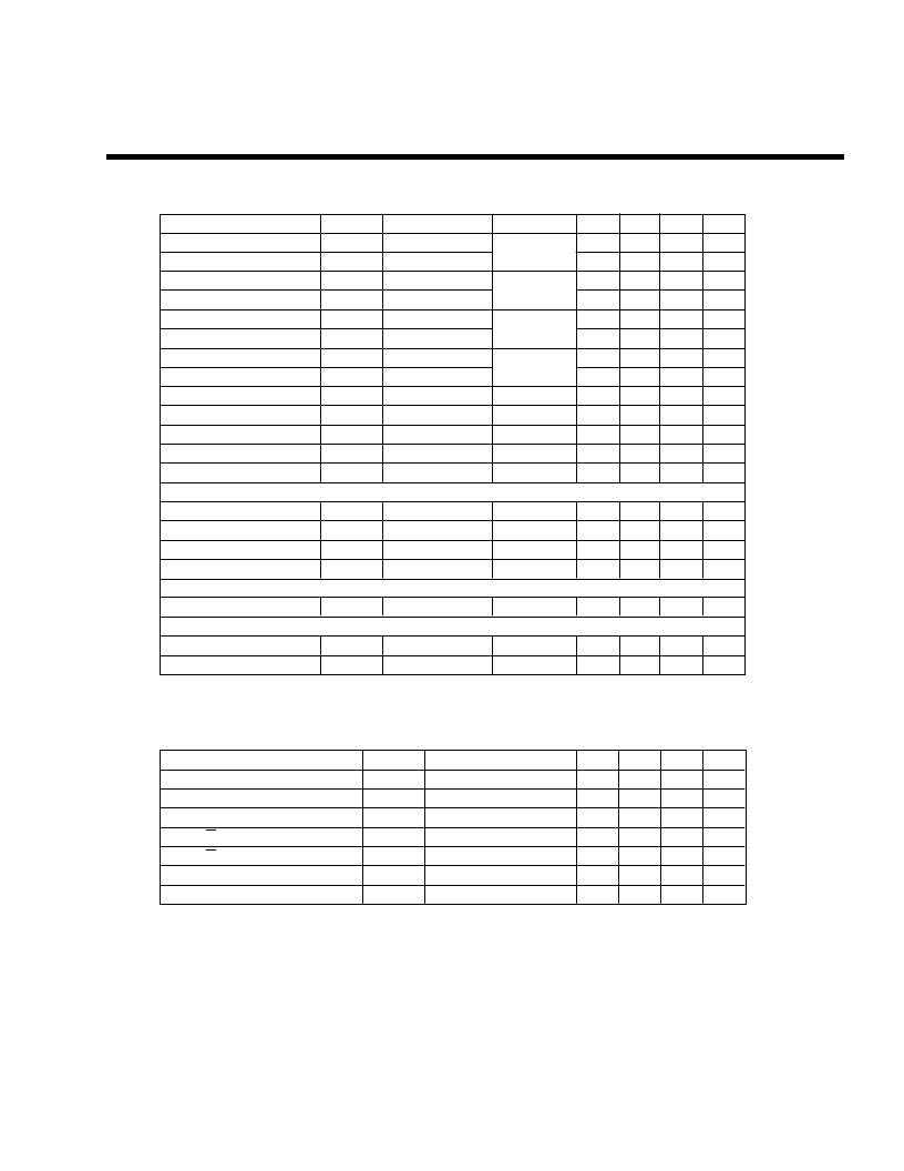
290
Parameter
Symbol
V
IH1
V
IL1
V
IH2
V
IL2
V
OH1
V
OL1
V
OH2
V
OL2
R
COM
R
SEG
I
IL
–I
P
I
op
Condition
Applicable Pin
DB0~DB7
RS, R/W, E
Min
2.0
V
SS
Typ
—
—
—
—
—
—
—
—
2
2.5
—
125
0.5
Max
V
DD
0.8
V
DD
1.0
—
0.4
—
0.1V
DD
10
10
1
250
0.8
Unit
V
V
V
V
V
V
V
V
k
k
μ
A
μ
A
mA
“H” level input voltage (1)
“L” level input voltage (1)
“H” level input voltage (2)
“L” level input voltage (2)
“H” level output voltage (1)
“L” level output voltage (1)
“H” level output voltage (2)
“L” level output voltage (2)
Driver-on resistor (COM)
Driver-on resistor (SEG)
I/O leakage current
Pull-up MOS current
Supply current
External clock operation
OSC1
V
DD
–1.0
V
SS
2.4
—
0.9V
DD
—
—
—
—
50
—
I
OH
=–0.205mA
I
OL
=1.6mA
I
OH
=–0.04mA
I
OL
=0.04mA
|V
COM
–V
n
|=0.5V
|V
SEG
–V
n
|=0.5V
V
I
=0 to V
DD
V
DD
=5V
Rf oscillation, from external clock
V
DD
=5V, f
OSC
=f
CP
=270kHz
DB0~DB7
COM1~16
SEG1~40
V
DD
External clock operating frequency
External clock duty
External clock rise time
External clock fall time
Internal clock operation (Rf oscillation)
Oscillation frequency
Internal clock operation (Ceramic filter oscillation)
Oscillation frequency
LCD driving voltage
f
EXTCL
Duty
tr
EXTCL
tf
EXTCL
125
45
—
—
250
50
—
—
350
55
0.2
0.2
kHz
%
μ
s
μ
s
f
OSC
R
f
=91k
±
2%
190
270
350
kHz
f
OSC
V
LCD
Ceramic filter
V
DD
–V5
245
3.0
250
—
255
V
DD
kHz
V
DC Characteristics
XSCL
LP
D0
(V
DD
= 5.0V
±
10%, V
SS
= 0V, T
a
= –20 to 75
°
C)
AC Characteristics
°
Read cycle
Parameter
Symbol
t
cycE
t
WEH
t
rE
, t
fE
t
AS
t
AH
t
RD
t
DHR
Conditions
Min
500
220
—
40
10
—
20
Typ
—
—
—
—
—
—
—
Max
—
—
25
—
—
120
—
Unit
ns
ns
ns
ns
ns
ns
ns
Enable cycle time
Enable “H” level pulse width
Enable rise/fall time
RS, R/W setup time
RS, R/W address hold time
Read data output delay
Read data hold time
C
L
=100pF
(V
DD
= 5.0V
±
10%, V
SS
= 0V, T
a
= –20 to 75
°
C)
SED1278
相關PDF資料 |
PDF描述 |
|---|---|
| SED1681F | CMOS DOT MATRIX LCD CONTROLLER DRIVER |
| SED1330 | CMOS GRAPHIC LCD CONTROLLER |
| SED1330F | CMOS GRAPHIC LCD CONTROLLER |
| SED1335-1 | CMOS GRAPHIC LCD CONTROLLER |
| SED1335 | LCD Controller ICs |
相關代理商/技術參數 |
參數描述 |
|---|---|
| SED1278FOB | 制造商:EPSON 制造商全稱:EPSON 功能描述:Dot Matrix LCD Controller Driver |
| SED1278FOC | 制造商:EPSON 制造商全稱:EPSON 功能描述:Dot Matrix LCD Controller Driver |
| SED1278FOD | 制造商:EPSON 制造商全稱:EPSON 功能描述:Dot Matrix LCD Controller Driver |
| SED1278FOG | 制造商:EPSON 制造商全稱:EPSON 功能描述:Dot Matrix LCD Controller Driver |
| SED1278FOH | 制造商:EPSON 制造商全稱:EPSON 功能描述:Dot Matrix LCD Controller Driver |
發(fā)布緊急采購,3分鐘左右您將得到回復。