- 您現(xiàn)在的位置:買賣IC網(wǎng) > PDF目錄192742 > SD-14621FS-154 (DATA DEVICE CORP) SYNCHRO OR RESOLVER TO DIGITAL CONVERTER, CDFP54 PDF資料下載
參數(shù)資料
| 型號(hào): | SD-14621FS-154 |
| 廠商: | DATA DEVICE CORP |
| 元件分類: | 位置變換器 |
| 英文描述: | SYNCHRO OR RESOLVER TO DIGITAL CONVERTER, CDFP54 |
| 封裝: | 1.500 X 0.780 INCH, 0.210 INCH HEIGHT, CERAMIC, FP-54 |
| 文件頁數(shù): | 12/12頁 |
| 文件大小: | 150K |
| 代理商: | SD-14621FS-154 |
9
Data Device Corporation
www.ddc-web.com
SD-14620
J-04/03-0
0.780 MAX
(19.81)
0.400
(10.16)
1.300 (33.02)
INDEX
DENOTES
PIN 1
0.210 MAX (5.33)
1.500 MAX
(36.75)
1.200 (30.48)
0.160 MIN
(4.06)
0.050
(1.27)
0.100 TYP (2.54)
0.050 TYP (1.27)
0.600
(15.24)
0.018
DIA TYP
(0.46)
26
27
28
29
53
54
2
1
3
52
30
25
NUMBERS FOR
REFERENCE ONLY
0.008
(0.20)
0.05
(1.27)
BOTTOM VIEW
SIDE VIEW
Notes:
1. Dimensions are in inches (mm).
2. Lead identification numbers are for reference only
3. Lead cluster shall be centered within ±0.005 (0.13) of outline dimensions.
Lead spacing dimensions apply only at seating plane.
4. Pin material meets solderability requirements to MIL-STD-202E, Method 208C.
5. Case is hermetically sealed ceramic package.
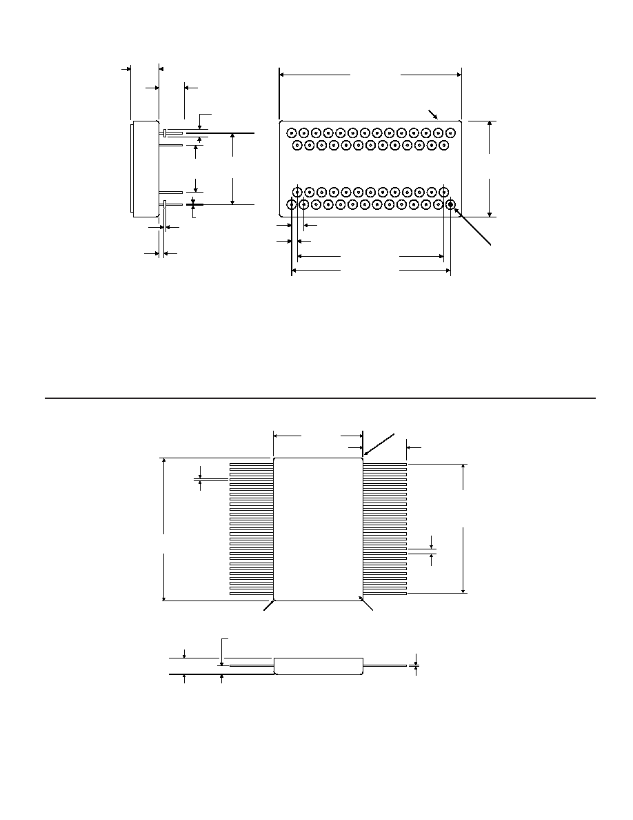
FIGURE 7. SD-14620 DIP MECHANICAL OUTLINE
26 EQ. SP. @
0.050 = 1.30
TOL NONCOM TYP
(1.24 = 33.02)
SEE NOTE 2
0.500 MIN TYP
(12.7)
0.100 ±0.010 TYP
(2.54 ±0.25)
0.210 MAX (5.33)
28
27
54
1
0.780 MAX
(19.81)
PIN 1 DENOTED BY
INDEX MARK
1.500 MAX
(38.1)
0.010 ±0.002 TYP
(0.25 ±0.05)
PIN NUMBERS FOR
REFERENCE ONLY
0.018 ±0.002 TYP
(0.46 ±0.05)
0.050 TYP
(1.27)
0.020 R TYP
(0.51)
BOTTOM VIEW
SIDE VIEW
Notes:
1. Dimensions are in inches (mm).
2. Lead cluster shall be centralized about case centerline within ±0.010 (±0.254).
FIGURE 8. SD-14620 FLAT PACK MECHANICAL OUTLINE
相關(guān)PDF資料 |
PDF描述 |
|---|---|
| SD-14621FS-155K | SYNCHRO OR RESOLVER TO DIGITAL CONVERTER, CDFP54 |
| SD-14621FS-155S | SYNCHRO OR RESOLVER TO DIGITAL CONVERTER, CDFP54 |
| SD-14621FS-155Z | SYNCHRO OR RESOLVER TO DIGITAL CONVERTER, CDFP54 |
| SD-14621FS-162K | SYNCHRO OR RESOLVER TO DIGITAL CONVERTER, CDFP54 |
| SD-14621FS-162Q | SYNCHRO OR RESOLVER TO DIGITAL CONVERTER, CDFP54 |
相關(guān)代理商/技術(shù)參數(shù) |
參數(shù)描述 |
|---|---|
| SD-14621FS-295 | 制造商:DDC 功能描述: |
| SD1463 | 制造商:STMICROELECTRONICS 制造商全稱:STMicroelectronics 功能描述:RF & MICROWAVE TRANSISTORS VHF/UHF APPLICATIONS |
| SD1468 | 制造商:MICROSEMI 制造商全稱:Microsemi Corporation 功能描述:RF AND MICROWAVE TRANSISTORS WIDEBAND VHF-UHF CLASS C |
| SD14-680 | 制造商:COOPER BUSSMANN 功能描述:Inductor Power Shielded Wirewound 68uH 20% 100KHz Ferrite 474mA 1.11Ohm DCR 2020 T/R 制造商:COOPER BUSSMANN 功能描述:Ind Power Shielded Wirewound 68uH 20% 100KHz Ferrite 474mA 2020 T/R |
| SD14-680-R | 功能描述:固定電感器 68uH 0.449A 1.11ohms RoHS:否 制造商:AVX 電感:10 uH 容差:20 % 最大直流電流:1 A 最大直流電阻:0.075 Ohms 工作溫度范圍:- 40 C to + 85 C 自諧振頻率:38 MHz Q 最小值:40 尺寸:4.45 mm W x 6.6 mm L x 2.92 mm H 屏蔽:Shielded 端接類型:SMD/SMT 封裝 / 箱體:6.6 mm x 4.45 mm |
發(fā)布緊急采購,3分鐘左右您將得到回復(fù)。