- 您現(xiàn)在的位置:買賣IC網(wǎng) > PDF目錄385820 > SCN2661CA1F28 (NXP SEMICONDUCTORS) SM Series Subminiature Basic Switch, Single Pole Double Throw (SPDT), 250 Vac, 5 A, Pin Plunger Actuator, Solder Termination PDF資料下載
參數(shù)資料
| 型號: | SCN2661CA1F28 |
| 廠商: | NXP SEMICONDUCTORS |
| 元件分類: | 微控制器/微處理器 |
| 英文描述: | SM Series Subminiature Basic Switch, Single Pole Double Throw (SPDT), 250 Vac, 5 A, Pin Plunger Actuator, Solder Termination |
| 中文描述: | 1 CHANNEL(S), 1M bps, SERIAL COMM CONTROLLER, CDIP28 |
| 封裝: | 0.600 INCH, CERAMIC, DIP-28 |
| 文件頁數(shù): | 7/19頁 |
| 文件大?。?/td> | 131K |
| 代理商: | SCN2661CA1F28 |
Philips Semiconductors
Product specification
SCN2661/SCN68661
Enhanced programmable communications
interface (EPCI)
1994 Apr 27
7
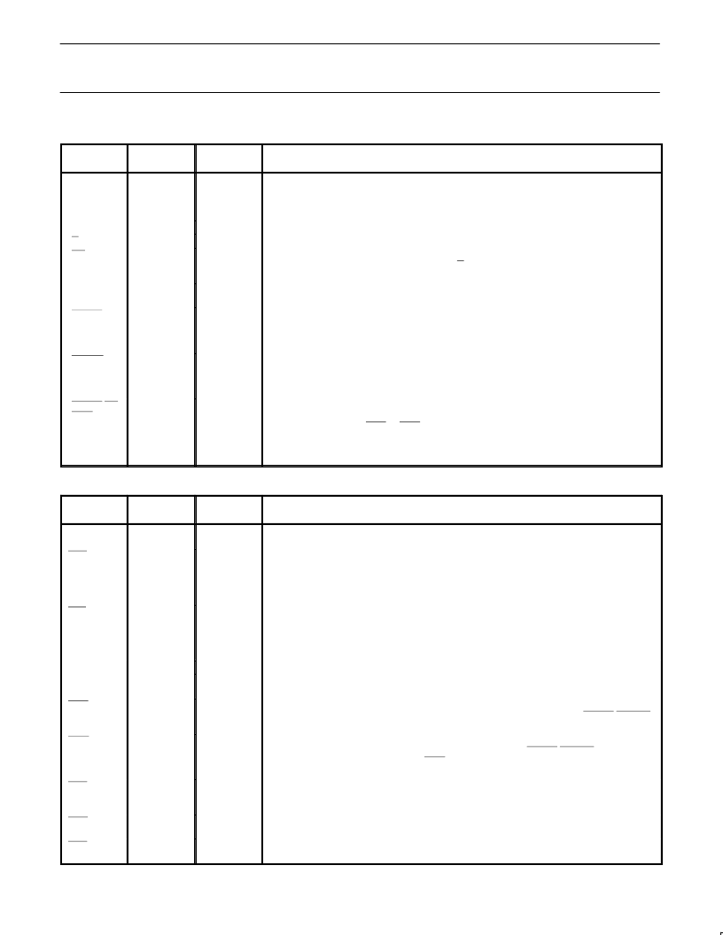
Table 2.
CPU-Related Signals
PIN NAME
PIN NO.
INPUT/
OUTPUT
FUNCTION
RESET
21
I
A High on this input performs a master reset on the 68661. This signal asynchronously
terminates any device activity and clears the mode, command and status registers. The
device assumes the idle state and remains there until initialized with the appropriate control
words.
Address lines used to select internal EPCI registers.
Read command when Low, write command when High.
Chip enable command. When Low, indicates that control and data lines to the EPCI are
valid and that the operation specified by the RW, A1 and A0 inputs should be performed.
When High, places the D0–D7 lines in the 3-State condition.
8-bit, 3-State data bus used to transfer commands, data and status between EPCI and the
CPU. D0 is the least significant bit, D7 the most significant bit.
This output is the complement of status register bit SR0. When Low, it indicates that the
transmit data holding register (THR) is ready to accept a data character from the CPU. It
goes High when the data character is loaded. This output is valid only when the transmitter
is enabled. It is an open-drain output which can be used as an interrupt to the CPU.
This output is the complement of status register bit SR1. When Low, it indicates that the
receive data holding register (RHR) has a character ready for input to the CPU. It goes
High when the RHR is read by the CPU, and also when the receiver is disabled. It is an
open-drain output which can be used as an interrupt to the CPU.
This output is the complement of status register bit SR2. When Low, it indicates that the
transmitter has completed serialization of the last character loaded by the CPU, or that a
change of state of the DSR or DCD inputs has occurred. This output goes High when the
status register is ready by the CPU, if the TxEMT condition does not exist. Otherwise, the
THR must be loaded by the CPU for this line to go high. It is an open-drain output which
can be used as an interrupt to the CPU. See Status Register (SR2) for details.
A0, A1
R/W
CE
12,10
13
11
I
I
I
D0–D7
27,28,1,2,5–8
I/O
TxRDY
15
O
RxRDY
14
O
TxEMT/DS
CHG
18
O
Table 3.
Device-Related Signals
PIN NAME
PIN NO.
INPUT/
OUTPUT
FUNCTION
BRCLK
20
I
Clock input to the internal baud rate generator (see Table 1). Not required if external
receiver and transmitter clocks are used.
Receiver clock. If external receiver clock is programmed, this input controls the rate at
which the character is to be received. Its frequency is 1X, 16X or 64X the baud rate, as
programmed by mode register 1. Data are sampled on the rising edge of the clock. If
internal receiver clock is programmed, this pin can be a 1X/16X clock or a break detect
output pin.
Transmitter clock. If external transmitter clock is programmed, this input controls the rate at
which the character is transmitted. Its frequency is 1X, 16X or 64X the baud rate, as
programmed by mode register 1. The transmitted data changes on the falling edge of the
clock. If internal transmitter clock is programmed, this pin can be a 1X/16X clock output or
an external jam synchronization input.
Serial data input to the receiver. “Mark” is High, “space” is Low.
Serial data output from the transmitter. “Mark” is High, “Space” is Low. Held in mark
condition when the transmitter is disabled.
General purpose input which can be used for data set ready or ring indicator condition. Its
complement appears as status register bit SR7. Causes a Low output on TxEMT/DSCHG
when its state changes if CR2 or CR0 = 1.
Data carrier detect input. Must be Low in order for the receiver to operate. Its complement
appears as status register bit SR6. Causes a Low output on TxEMT/DSCHG when its
state changes if CR2 or CR0 = 1. If DCD goes High while receiving, the RxC is internally
inhibited.
Clear to send input. Must be Low in order for the transmitter to operate. If it goes High
during transmission, the character in the transmit shift register will be transmitted before
termination.
General purpose output which is the complement of command register bit CR1. Normally
used to indicate data terminal ready.
General purpose output which is the complement of command register bit CR5. Normally
used to indicate request to send. See Command Register (CR5) for details.
RxC/BKDET
25
I/O
TxC/XSYNC
9
I/O
RxD
TxD
3
19
I
O
DSR
22
I
DCD
16
I
CTS
17
I
DTR
24
O
RTS
23
O
相關(guān)PDF資料 |
PDF描述 |
|---|---|
| SCN2661CC1A28 | Enhanced programmable communications interface EPCI |
| SCN2661CC1F28 | SM Series Subminiature Basic Switch, Single Pole Double Throw (SPDT), 125 Vac, 1 A, Pin Plunger Actuator, Solder Termination |
| SCN2661CC1N28 | Enhanced programmable communications interface EPCI |
| SCOCXOT | 12V OCXO HCMOS Output 14-pin DIL |
| SCOCXOT-AR1 | 12V OCXO HCMOS Output 14-pin DIL |
相關(guān)代理商/技術(shù)參數(shù) |
參數(shù)描述 |
|---|---|
| SCN2661CC1A28 | 制造商:PHILIPS 制造商全稱:NXP Semiconductors 功能描述:Enhanced programmable communications interface EPCI |
| SCN2661CC1F28 | 制造商:PHILIPS 制造商全稱:NXP Semiconductors 功能描述:Enhanced programmable communications interface EPCI |
| SCN2661CC1N28 | 制造商:PHILIPS 制造商全稱:NXP Semiconductors 功能描述:Enhanced programmable communications interface EPCI |
| SCN2672AC4N40 | 制造商:North American Philips Discrete Products Div 功能描述:NON-VGA VIDEO CONTROLLER, 40 Pin, DIP |
| SCN2674 | 制造商:未知廠家 制造商全稱:未知廠家 功能描述:Advanced Video Display Controller (AVDC) |
發(fā)布緊急采購,3分鐘左右您將得到回復(fù)。