- 您現(xiàn)在的位置:買賣IC網(wǎng) > PDF目錄372130 > SCN2651 (NXP Semiconductors N.V.) Programmable communications interface PCI PDF資料下載
參數(shù)資料
| 型號: | SCN2651 |
| 廠商: | NXP Semiconductors N.V. |
| 英文描述: | Programmable communications interface PCI |
| 中文描述: | 可編程通信接口的PCI |
| 文件頁數(shù): | 6/15頁 |
| 文件大小: | 118K |
| 代理商: | SCN2651 |
Philips Semiconductors
Product specification
SCN2651
Programmable communications interface (PCI)
1994 Apr 27
6
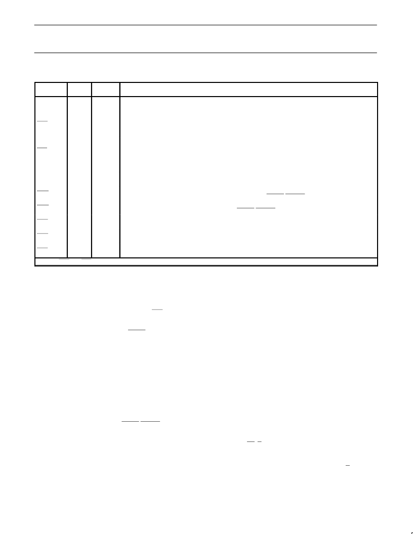
Table 3.
Device-Related Signals
PIN
NO.
UTPUT
PIN NAME
INPUT/O
FUNCTION
BRCLK
20
I
5.0688MHz clock input to the internal baud rate generator. Not required if external receiver and
transmitter clocks are used.
Receiver clock. If external receiver clock is programmed, this input controls the rate at which the
character is to be received. Its frequency is 1X, 16X or 64X the baud rate, as programmed by mode
register 1. Data are sampled on the rising edge of the clock. If internal receiver clock is programmed, this
pin becomes an output at 1X the programmed baud rate.*
Transmitter clock. If external transmitter clock is programmed, this input controls the rate at which the
character is transmitted. Its frequency is 1X, 16X or 64X the baud rate, as programmed by mode register
1. The transmitted data changes on the falling edge of the clock. If internal transmitter clock is
programmed, the pin becomes an output at 1X the programmed baud rate.*
Serial data input to the receiver. “Mark” is high, “Space” is low.
Serial data output from the transmitter. “Mark” is high, “space” is low. Held in mark condition when the
transmitter is disabled.
General purpose input which can be used for data set ready or ring indicator condition. Its complement
appears as status register bit SR7. Causes a low output on TxEMT/DSCHG when its state changes.
Data carrier detect input. Must be low in order for the receiver to operate. Its complement appears as
status register bit SR6. Causes a low output on TxEMT/DSCHG when its state changes.
Clear to send input. Must be low in order for the transmitter to operate. If it goes high during
transmission, the character in the transmit shift register will be transmitted before termination.
General purpose output which is the complement of command register bit CR1. Normally used to indicate
data terminal ready.
General purpose output which is the complement of command register bit CR5. Normally used to indicate
request to send.
NOTE:
*RxC and TxC outputs have short circuit protection max. C
L
= 100pF
RxC
25
I/O
TxC
9
I/O
RxD
3
I
TxD
19
O
DSR
22
I
DCD
16
I
CTS
17
I
DTR
24
O
RTS
23
O
commanded, SYN characters are not transferred to the Holding
Register. Note that the SYN characters used to establish initial
synchronization are not transferred to the holding register in any
case.
Transmitter
The PCI is conditioned to transmit data when the CTS input is Low
and the TxEN command register bit is set. The SCN2651 indicates
to the CPU that it can accept a character for transmission by setting
the TxRDY status bit and asserting the TxRDY output. When the
CPU writes a character into the transmit data holding register, these
conditions are negated. Data is transferred from the holding register
to the transmit shift register when it is idle or has completed
transmission of the previous character. The TxRDY conditions are
then asserted again. Thus, one full character time of buffering is
provided.
In the asynchronous mode, the transmitter automatically sends a
start bit followed by the programmed number of data bits, the least
significant bit being sent first. It then appends an optional odd or
even parity bit and the programmed number of stop bits. If,
following transmission of the data bits, a new character is not
available in the transmit holding register, the TxD output remains in
the marking (high) condition and the TxEMT/DSCHG output and its
corresponding status bit are asserted. Transmission resumes when
the CPU loads a new character into the holding register. The
transmitter can be forced to output a continuous low (BREAK)
condition by setting the send break command bit high.
In the synchronous mode, when the SCN2651 is initially conditioned
to transmit, the TxD output remains high and the TxRDY condition is
asserted until the first character to be transmitted (usually a SYN
character) is loaded by the CPU. Subsequent to this, a continuous
stream of characters is transmitted. No extra bits (other than parity,
if commanded) are generated by the PCI unless the CPU fails to
send a new character to the PCI by the time the transmitter has
completed sending the previous character.
Since synchronous communication does not allow gaps between
characters, the PCI asserts TxEMT and automatically “fills” the gap
by transmitting SYN1s, SYN1–SYN2 doublets, or DLE–SYN1
doublets, depending on the state of MR16 and MR17. Normal
transmission of the message resumes when a new character is
available in the transmit data holding register. If the send DLE bit in
the command register is true, the DLE character is automatically
transmitted prior to transmission of the message character in the
THR.
PCI PROGRAMMING
Prior to initiating data communications, the SCN2651 operational
mode must be programmed by performing write operations to the
mode and command registers. In addition, if synchronous operation
is programmed, the appropriate SYN/DLE registers must be loaded.
The PCI can be reconfigured at any time during program execution.
However, if the change has an effect on the reception of a character
the receiver should be disabled. Alternatively if the change is made
1 1/2 RxC periods after RxRDY goes active it will affect the next
character assembly. A flowchart of the initialization process appears
in Figure 1.
The internal registers of the PCI are accessed by applying specific
signals to the CE, R/W, A
1
and A
0
inputs. The conditions necessary
to address each register are shown in Table 4.
The SYN1, SYN2, and DLE registers are accessed by performing
write operations with the conditions A
1
= 0, A
0
= 1, and R/W = 1.
The first operation loads the SYN1 register. The next loads the
SYN2 register, and the third loads the DLE register. Reading or
loading the mode registers is done in a similar manner. The first
write (or read) operation addresses mode register 1, and a
subsequent operation addresses mode register 2. If more than the
相關(guān)PDF資料 |
PDF描述 |
|---|---|
| SCN2651CC1N28 | Programmable communications interface PCI |
| SCN2652 | Multi-protocol communications controller MPCC |
| SCN2652AC2A44 | NT Series Toggle Switch, 1 pole, 3 position, Solder terminal, Locking Lever |
| SCN2652AC2N40 | Multi-protocol communications controller MPCC |
| SCN68652 | Multi-protocol communications controller MPCC |
相關(guān)代理商/技術(shù)參數(shù) |
參數(shù)描述 |
|---|---|
| SCN2651C1N28 | 制造商:North American Philips Discrete Products Div 功能描述:1 CHANNEL(S), 1M bps, SERIAL COMM CONTROLLER, PDIP28 |
| SCN2651CC1I28 | 制造商:NXP Semiconductors 功能描述:IC,COMMUNICATIONS INTERFACE,MOS,DIP,28PIN,CERAMIC |
| SCN2651CC1N28 | 制造商:NXP Semiconductors 功能描述:COMMUNICATIONS INTERFACE, 28 Pin, Plastic, DIP |
| SCN2652 | 制造商:PHILIPS 制造商全稱:NXP Semiconductors 功能描述:Multi-protocol communications controller MPCC |
| SCN2652AC1I40 | 制造商:North American Philips Discrete Products Div 功能描述:COMMUNICATIONS INTERFACE, 40 Pin, Ceramic, DIP |
發(fā)布緊急采購,3分鐘左右您將得到回復(fù)。