- 您現(xiàn)在的位置:買(mǎi)賣(mài)IC網(wǎng) > PDF目錄383804 > SCANPSC100FSC (FAIRCHILD SEMICONDUCTOR CORP) Embedded Boundary Scan Controller (IEEE 1149.1 Support) PDF資料下載
參數(shù)資料
| 型號(hào): | SCANPSC100FSC |
| 廠商: | FAIRCHILD SEMICONDUCTOR CORP |
| 元件分類: | 微控制器/微處理器 |
| 英文描述: | Embedded Boundary Scan Controller (IEEE 1149.1 Support) |
| 中文描述: | SPECIALTY MICROPROCESSOR CIRCUIT, PDSO28 |
| 封裝: | 0.300 INCH, MS-013, SOIC-28 |
| 文件頁(yè)數(shù): | 7/21頁(yè) |
| 文件大小: | 208K |
| 代理商: | SCANPSC100FSC |
第1頁(yè)第2頁(yè)第3頁(yè)第4頁(yè)第5頁(yè)第6頁(yè)當(dāng)前第7頁(yè)第8頁(yè)第9頁(yè)第10頁(yè)第11頁(yè)第12頁(yè)第13頁(yè)第14頁(yè)第15頁(yè)第16頁(yè)第17頁(yè)第18頁(yè)第19頁(yè)第20頁(yè)第21頁(yè)
7
www.fairchildsemi.com
S
Parallel Processor Interface (PPI)
(Continued)
TIMING WAVEFORMS (Continued)
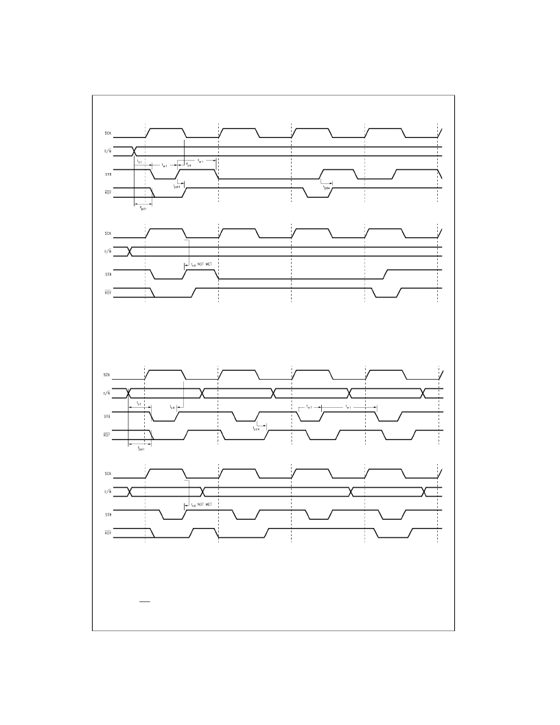
FIGURE 4. Consecutive Read/Writes (best case timing)
FIGURE 5. Consecutive Read/Writes (worst case timing)
Note 3: Figures 4, 5:
Figure 4 shows the best case bus cycle timing for SCK and STB during consecutive read or write cycles. The rising edge of strobe
occurs a setup time, t
S4
or before the falling edge of SCK. This allows the cycle to be completed within 1.5 clock SCK clock cycles. Figure 5 shows the worst
case bus cycle timing for SCK and STB during consecutive read or write cycles. The rising edge of strobe does not meet the t
S4
requirement between STB
and SCK. Therefore, the propagation of the internal PSC100 control and reset signals is delayed until the next falling edge of SCK. The bus cycle is then
completed 1.5 SCK cycles later creating a total bus cycle time of 2.5 SCK cycles. If worst case timing is considered for bus cycle timing, t
S4
is not a manda-
tory timing specification.
FIGURE 6. Read/Write or Write/Read (best case timing)
FIGURE 7. Read/Write or Write/Read (worst case timing)
Note 4:
Figures 6, 7: This diagram shows the timing for a read followed by a write (or write followed by a read). Separate Read and Write data/address
latches and control logic allow consecutive read/write or write/read operations to be overlapped (i.e., do not need to wait 2 or 3 SCK cycles between bus
cycles). For the best case timing scenario (Figure 6: rising edge of STB to falling edge of SCK greater than t
S4
), a new bus cycle can be performed each SCK
cycle. For the worst timing scenario (Figure 7: rising edge of STB to falling edge of SCK is less than t
S4
), a one SCK cycle delay must be included after each
back to back read/write or write/read sequence.
Note 5:
Figures 4, 5, 6, 7 assume that the PSC100 register participating in the bus cycle is ready to accept/provide data. For bus cycles involving a PSC100
shifter/buffer(s), the ready status of a shifter/buffer can be checked using the status bits in Mode Register 2 prior to the start of the bus cycle. Polling is
required when the RDY pin is not used to provide a processor
“
handshake
”
.
相關(guān)PDF資料 |
PDF描述 |
|---|---|
| SCANPSC110FSC | SCAN Bridge Hierarchical and Multidrop Addressable JTAG Port (IEEE1149.1 System Test Support) |
| SCP-5453 | SOCKET,IC,16PIN,MACHINE TOOLED WIRE WRAP,0.3"WIDE,0.515"LEAD |
| SCP-6122 | POWER OPERATIONAL AMPLIFIER |
| SCS152 | HM Series Hermetically Sealed Basic Switch, Single Pole Double Throw Circuitry, 0.5 A at 28 Vdc, Integral Lever Actuator, Solder Termination |
| SCS152-IS | Small glass bead with axial leads |
相關(guān)代理商/技術(shù)參數(shù) |
參數(shù)描述 |
|---|---|
| SCANPSC100FSCX | 功能描述:接口 - 專用 Emb Boun Scan Cont RoHS:否 制造商:Texas Instruments 產(chǎn)品類型:1080p60 Image Sensor Receiver 工作電源電壓:1.8 V 電源電流:89 mA 最大功率耗散: 最大工作溫度:+ 85 C 安裝風(fēng)格:SMD/SMT 封裝 / 箱體:BGA-59 |
| SCANPSC110 | 制造商:NSC 制造商全稱:National Semiconductor 功能描述:SCAN Bridge Hierarchical and Multidrop Addressable JTAG Port (IEEE1149.1 System Test Support) |
| SCANPSC110_ZFC3026B WAF | 制造商:Fairchild Semiconductor Corporation 功能描述: |
| SCANPSC110F | 制造商:NSC 制造商全稱:National Semiconductor 功能描述:SCAN Bridge Hierarchical and Multidrop Addressable JTAG Port (IEEE1149.1 System Test Support) |
| SCANPSC110FDMQB | 制造商:NSC 制造商全稱:National Semiconductor 功能描述:SCAN Bridge Hierarchical and Multidrop Addressable JTAG Port (IEEE1149.1 System Test Support) |
發(fā)布緊急采購(gòu),3分鐘左右您將得到回復(fù)。