- 您現在的位置:買賣IC網 > PDF目錄374727 > SC411 (Semtech Corporation) Synchronous Buck Pseudo-Fixed Frequency Power Supply Controller PDF資料下載
參數資料
| 型號: | SC411 |
| 廠商: | Semtech Corporation |
| 英文描述: | Synchronous Buck Pseudo-Fixed Frequency Power Supply Controller |
| 中文描述: | 同步降壓偽固定頻率電源控制器 |
| 文件頁數: | 17/27頁 |
| 文件大小: | 488K |
| 代理商: | SC411 |
第1頁第2頁第3頁第4頁第5頁第6頁第7頁第8頁第9頁第10頁第11頁第12頁第13頁第14頁第15頁第16頁當前第17頁第18頁第19頁第20頁第21頁第22頁第23頁第24頁第25頁第26頁第27頁
17
2007 Semtech Corp.
www.semtech.com
SC411
POWER MANAGEMENT
Layout Guidelines
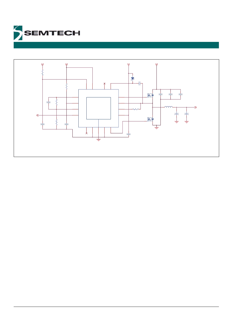
Figure 4: Reference Design
One (or more) ground planes is/are recommended to minimize the effect of switching noise and copper losses, and
maximize heat dissipation. The IC ground reference, VSSA, and the power ground pin, PGND, should both connect
directly to the device thermal pad. The thermal pad should connect to the ground plane(s) using multiple vias.
The VOUT feedback trace must be kept far away from noise sources such as switching nodes, inductors and gate
drives. Route the feedback trace in a quiet layer (if possible) from the output capacitor back to the chip. All compo-
nents should be located adjacent to their respective pins with an emphasis on the chip decoupling capacitors (VCCA
and VDDP) and the components that are shown connecting to VSSA in the above schematic. Make any ground con-
nections simply to the ground plane.
Power sections should connect directly to the ground plane(s) using multiple vias as required for current handling (in-
cluding the chip power ground connections). Power components should be placed to minimize loops and reduce loss-
es. Make all the connections on one side of the PCB using wide copper
fi
lled areas if possible. Do not use “minimum”
land patterns for power components. Minimize trace lengths between the gate drivers and the gates of the MOSFETs
to reduce parasitic impedances (and MOSFET switching losses), the low-side MOSFET is most critical. Maintain a
length to width ratio of <20:1 for gate drive signals. Use multiple vias as required by current handling requirements
(and to reduce parasitics) if routed on more than one layer. Current sense connections must always be made using
Kelvin connections to ensure an accurate signal, with the current limit resistor located at the device.
We will examine the reference design used in the Design Procedure section while explaining the layout guidelines in
more detail.
VOUT
C8
1nF
0402
VBAT
R1
1M
0402
PGOOD
Q1
IRF7811AV
C10
1uF
0603
R4
7k87
C1
0u1
D1
SOD323
C2
2n2/50V
0402
VBAT
5VSUS
L1
2u2
+
C6
220u/25m
7343
VOUT
R2
10R
0402
5VSUS
VOUT
1
VCCA
2
FB
3
PGD
4
N
5
V
6
P
7
D
8
VDDP
9
ILIM
10
LX
11
DH
12
B
1
N
1
E
1
T
1
T
U1
SC411
Q2
FDS6676S
C5
56p
0402
0402
0402
0603
0402
0603
C3
0u1/25V
0603
C4
10u/25V
1210
+
C7
220u/25m
7343
VBAT = 8V to 20V
VOUT = 1.2V @ 6A
C9
1uF
R3
20k0
R5
14k3
相關PDF資料 |
PDF描述 |
|---|---|
| SC411EVB | Synchronous Buck Pseudo-Fixed Frequency Power Supply Controller |
| SC411MLTRT | Synchronous Buck Pseudo-Fixed Frequency Power Supply Controller |
| SC412A | Synchronous Buck Controller |
| SC412AEVB | Synchronous Buck Controller |
| SC412AMLTRT | Synchronous Buck Controller |
相關代理商/技術參數 |
參數描述 |
|---|---|
| SC411201B | 制造商:Freescale Semiconductor 功能描述:MOTSC411201B ACCTON:110000000028H |
| SC411209B | 制造商:Freescale Semiconductor 功能描述: |
| SC411212C | 制造商:Freescale Semiconductor 功能描述: |
| SC411EVB | 制造商:SEMTECH 制造商全稱:Semtech Corporation 功能描述:Synchronous Buck Pseudo-Fixed Frequency Power Supply Controller |
| SC411MLTRT | 制造商:Semtech Corporation 功能描述:Synchronous Buck Pseudo-Fixed Frequency Power Supply Controller |
發(fā)布緊急采購,3分鐘左右您將得到回復。