- 您現(xiàn)在的位置:買賣IC網(wǎng) > PDF目錄192316 > SC2612CMSTR (Semtech Corporation) 600kHz/200kHz Step-Down DC/DC Converter PDF資料下載
參數(shù)資料
| 型號: | SC2612CMSTR |
| 廠商: | Semtech Corporation |
| 英文描述: | 600kHz/200kHz Step-Down DC/DC Converter |
| 中文描述: | 600kHz/200kHz降壓型DC / DC轉換器 |
| 文件頁數(shù): | 9/12頁 |
| 文件大小: | 453K |
| 代理商: | SC2612CMSTR |
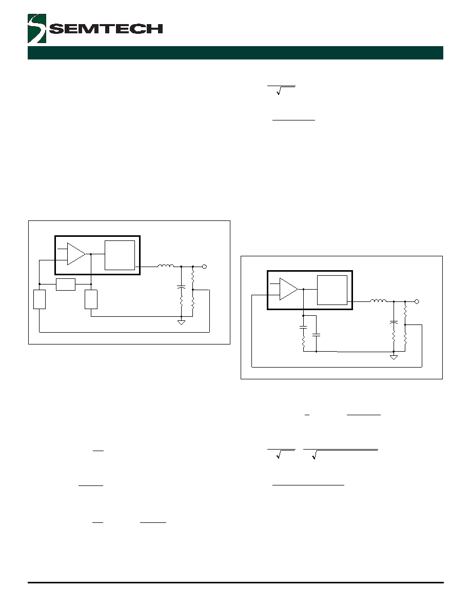
6
2003 Semtech Corp.
www.semtech.com
POWER MANAGEMENT
SC2612A/C
COMPENSA
COMPENSATION COMPONENTS
TION COMPONENTS
TION COMPONENTS - Once the filter com-
ponents have been determined, the compensation com-
ponents can be calculated. The goal of compensation is
to modify the frequency response characteristics of the
error amplifier to ensure that the closed loop feedback
system has the highest gain and bandwidth possible while
maintaining stability.
A simplified stability criteria states that the open loop
gain of the converter should fall through 0dB at 20dB/
decade at a frequency no higher than 20-25% of the
switching frequency.
This objective is most simply met by generating asymp-
totic bode plots of the small signal response of the vari-
ous sections of the converter.
L
VOUT
Co
SC2612 AND FETS
FB
OUT
COMP
Ra
MODULATOR
REF
+
-
EA
Rb
Resr
Zp
Zf
Zs
It is convenient to split the converter into two sections,
the Error amp and compensation components being one
section and the Modulator, output filter and divider be-
ing the other.
First calculate the DC Filter+Modulator+Divider gain
The DC filter gain is always 0dB, the Modulator gain is
19dB at 5V in and is proportional to Vin, so modulator
gain at any input voltage is.
÷
è
×
+
=
5
20
19
IN
MOD
V
Log
G
the divider gain is given by
÷÷
è
+
×
=
8
5
8
20
R
Log
G
DIV
So the total Filter+Modulator+Divider DC Gain is
÷÷
è
+
×
+
÷
è
×
+
=
B
A
B
IN
FMD
R
Log
V
Log
G
20
5
20
19
Calculate the filter double pole frequency (Fp(lc))
LCo
)
lc
(
Fp
p
=
2
1
and calculate ESR Zero frequency (Fz(esr))
sr
Re
Co
)
esr
(
Fz
×
p
=
2
1
Choose an open loop crossover frequency (Fco) no higher
than 20% of the switching frequency (Fs).
The proximity of Fz(esr) to the crossover frequency Fco
determines the type of compensation required, if
Fz(esr)>Fco/4, use type 3 compensation, otherwise use
type 2. Type 1 compensation is not appropriate and is
not discussed here.
Type 2 Example
As an example of type 2 compensation, we will use the
Evaluation board schematic.
3.3uH
VOUT
3000uF
SC2612 AND FETS
FB
OUT
COMP
6.98k
MODULATOR
REF
+
-
EA
8.06k
22mOhm
Cs
Cp
Rs
Vin=5V
The total Filter+Modulator+Divider DC Gain is
dB
.
Log
G
FMD
6
13
06
8
98
6
06
8
20
5
20
19
=
÷
è
+
×
+
÷
è
×
+
=
This is drawn as the line A-B in Fig2
kHz
.
LCo
)
lc
(
Fp
6
1
10
3000
10
3
2
1
2
1
6
×
p
=
p
=
-
This is point B in Fig2.
kHz
.
)
esr
(
Fz
4
2
10
22
10
3000
2
1
3
6
=
×
p
=
-
This is point C in Fig2., the line joining B-C slopes at -
40dB/decade, the line joining C-D slopes at -20dB/de-
cade.
For 600kHz switching frequency, crossover is designed
for 100kHz.
Since Fz(esr)<<Fco/4 Type 2 compensation is appropri-
ate.
相關PDF資料 |
PDF描述 |
|---|---|
| SC2612CMSTRT | 600kHz/200kHz Step-Down DC/DC Converter |
| SC311-6-TE12LA | 0.5 A, 600 V, SILICON, SIGNAL DIODE |
| SC40-19SEKWA | 7 SEG NUMERIC DISPLAY, SUPER BRIGHT ORANGE, 101.2 mm |
| SC40000 | RELAY SOCKET |
| SC40010 | RELAY SOCKET |
相關代理商/技術參數(shù) |
參數(shù)描述 |
|---|---|
| SC2612CMSTRT | 制造商:SEMTECH 制造商全稱:Semtech Corporation 功能描述:600kHz/200kHz Step-Down DC/DC Converter |
| SC2612E | 制造商:SEMTECH 制造商全稱:Semtech Corporation 功能描述:500kHz Step-Down DC/DC Converter |
| SC2612ES.TRT | 制造商:SEMTECH 功能描述:I.C. |
| SC2612ESTRT | 制造商:Semtech Corporation 功能描述:Conv DC-DC Single Step Down 4.5V to 15V 8-Pin SOIC T/R |
| SC2614ML.TR | 制造商:Semtech Corporation 功能描述: |
發(fā)布緊急采購,3分鐘左右您將得到回復。