- 您現(xiàn)在的位置:買賣IC網(wǎng) > PDF目錄98075 > SAF-XC2220L-20F66V (INFINEON TECHNOLOGIES AG) 32-BIT, FLASH, 66 MHz, RISC MICROCONTROLLER, PQCC48 PDF資料下載
參數(shù)資料
| 型號(hào): | SAF-XC2220L-20F66V |
| 廠商: | INFINEON TECHNOLOGIES AG |
| 元件分類: | 微控制器/微處理器 |
| 英文描述: | 32-BIT, FLASH, 66 MHz, RISC MICROCONTROLLER, PQCC48 |
| 封裝: | 0.50 MM PITCH, GREEN, PLASTIC, VQFN-48 |
| 文件頁數(shù): | 28/112頁 |
| 文件大?。?/td> | 3122K |
| 代理商: | SAF-XC2220L-20F66V |
第1頁第2頁第3頁第4頁第5頁第6頁第7頁第8頁第9頁第10頁第11頁第12頁第13頁第14頁第15頁第16頁第17頁第18頁第19頁第20頁第21頁第22頁第23頁第24頁第25頁第26頁第27頁當(dāng)前第28頁第29頁第30頁第31頁第32頁第33頁第34頁第35頁第36頁第37頁第38頁第39頁第40頁第41頁第42頁第43頁第44頁第45頁第46頁第47頁第48頁第49頁第50頁第51頁第52頁第53頁第54頁第55頁第56頁第57頁第58頁第59頁第60頁第61頁第62頁第63頁第64頁第65頁第66頁第67頁第68頁第69頁第70頁第71頁第72頁第73頁第74頁第75頁第76頁第77頁第78頁第79頁第80頁第81頁第82頁第83頁第84頁第85頁第86頁第87頁第88頁第89頁第90頁第91頁第92頁第93頁第94頁第95頁第96頁第97頁第98頁第99頁第100頁第101頁第102頁第103頁第104頁第105頁第106頁第107頁第108頁第109頁第110頁第111頁第112頁
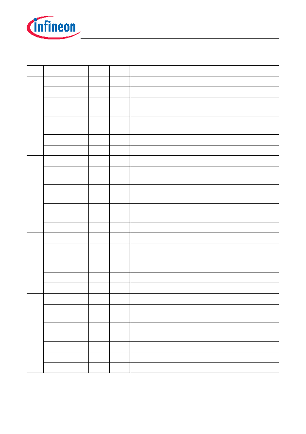
XC2220L, XC2224L
XC2000 Family / Econo Line
General Device Information
PRELIMINARY
Data Sheet
18
V1.0, 2010-12
32
P10.1
O0 / I St/B
Bit 1 of Port 10, General Purpose Input/Output
U0C0_DOUT O1
St/B
USIC0 Channel 0 Shift Data Output
CCU60_CC6
1
O2
St/B
CCU60 Channel 1 Output
CCU60_CC6
1INA
ISt/B
CCU60 Channel 1 Input
U0C0_DX0B
I
St/B
USIC0 Channel 0 Shift Data Input
U0C0_DX1A
I
St/B
USIC0 Channel 0 Shift Clock Input
33
P10.2
O0 / I St/B
Bit 2 of Port 10, General Purpose Input/Output
U0C0_SCLK
OUT
O1
St/B
USIC0 Channel 0 Shift Clock Output
CCU60_CC6
2
O2
St/B
CCU60 Channel 2 Output
CCU60_CC6
2INA
ISt/B
CCU60 Channel 2 Input
U0C0_DX1B
I
St/B
USIC0 Channel 0 Shift Clock Input
34
P10.3
O0 / I St/B
Bit 3 of Port 10, General Purpose Input/Output
CCU60_COU
T60
O2
St/B
CCU60 Channel 0 Output
U0C0_DX2A
I
St/B
USIC0 Channel 0 Shift Control Input
U0C1_DX2A
I
St/B
USIC0 Channel 1 Shift Control Input
RxDC1D
I
St/B
CAN Node 1 Receive Data Input
35
P10.4
O0 / I St/B
Bit 4 of Port 10, General Purpose Input/Output
U0C0_SELO
3
O1
St/B
USIC0 Channel 0 Select/Control 3 Output
CCU60_COU
T61
O2
St/B
CCU60 Channel 1 Output
U0C0_DX2B
I
St/B
USIC0 Channel 0 Shift Control Input
U0C1_DX2B
I
St/B
USIC0 Channel 1 Shift Control Input
ESR1_9
I
St/B
ESR1 Trigger Input 9
Table 6
Pin Definitions and Functions (cont’d)
Pin
Symbol
Ctrl.
Type Function
相關(guān)PDF資料 |
PDF描述 |
|---|---|
| SAF-XC2220L-20F80V | 32-BIT, FLASH, 80 MHz, RISC MICROCONTROLLER, PQCC48 |
| SAH-XC2220L-12F80V | 32-BIT, FLASH, 80 MHz, RISC MICROCONTROLLER, PQCC48 |
| SAH-XC2220L-20F66V | 32-BIT, FLASH, 66 MHz, RISC MICROCONTROLLER, PQCC48 |
| SAH-XC2224L-12F80V | 32-BIT, FLASH, 80 MHz, RISC MICROCONTROLLER, PQCC48 |
| SAK-XC2220L-12F80V | 32-BIT, FLASH, 80 MHz, RISC MICROCONTROLLER, PQCC48 |
相關(guān)代理商/技術(shù)參數(shù) |
參數(shù)描述 |
|---|---|
| SAF-XC2336A-56F80L AA | 功能描述:16位微控制器 - MCU 16Bit Sngl-Chip MCU w/32Bit Perform RoHS:否 制造商:Texas Instruments 核心:RISC 處理器系列:MSP430FR572x 數(shù)據(jù)總線寬度:16 bit 最大時(shí)鐘頻率:24 MHz 程序存儲(chǔ)器大小:8 KB 數(shù)據(jù) RAM 大小:1 KB 片上 ADC:Yes 工作電源電壓:2 V to 3.6 V 工作溫度范圍:- 40 C to + 85 C 封裝 / 箱體:VQFN-40 安裝風(fēng)格:SMD/SMT |
| SAF-XC2336A-72F80L AA | 功能描述:16位微控制器 - MCU 16Bit Sngl-Chip MCU w/32Bit Perform RoHS:否 制造商:Texas Instruments 核心:RISC 處理器系列:MSP430FR572x 數(shù)據(jù)總線寬度:16 bit 最大時(shí)鐘頻率:24 MHz 程序存儲(chǔ)器大小:8 KB 數(shù)據(jù) RAM 大小:1 KB 片上 ADC:Yes 工作電源電壓:2 V to 3.6 V 工作溫度范圍:- 40 C to + 85 C 封裝 / 箱體:VQFN-40 安裝風(fēng)格:SMD/SMT |
| SAF-XC2365-48F66L | 制造商:INFINEON 制造商全稱:Infineon Technologies AG 功能描述:16/32-Bit Single-Chip Microcontroller with 32-Bit Performance |
| SAF-XC2365-56F66L | 制造商:INFINEON 制造商全稱:Infineon Technologies AG 功能描述:16/32-Bit Single-Chip Microcontroller with 32-Bit Performance |
| SAF-XC2365-72F66L | 制造商:INFINEON 制造商全稱:Infineon Technologies AG 功能描述:16/32-Bit Single-Chip Microcontroller with 32-Bit Performance |
發(fā)布緊急采購,3分鐘左右您將得到回復(fù)。