- 您現(xiàn)在的位置:買賣IC網(wǎng) > PDF目錄372108 > SA8026DH (NXP SEMICONDUCTORS) ECONOLINE: RB & RA - Dual Output from a Single Input Rail- Power Sharing on Output- Industry Standard Pinout- 1kVDC & 2kVDC Isolation- Custom Solutions Available- UL94V-0 Package Material- Efficiency to 85% PDF資料下載
參數(shù)資料
| 型號: | SA8026DH |
| 廠商: | NXP SEMICONDUCTORS |
| 元件分類: | XO, clock |
| 英文描述: | ECONOLINE: RB & RA - Dual Output from a Single Input Rail- Power Sharing on Output- Industry Standard Pinout- 1kVDC & 2kVDC Isolation- Custom Solutions Available- UL94V-0 Package Material- Efficiency to 85% |
| 中文描述: | PLL FREQUENCY SYNTHESIZER, 2500 MHz, PDSO20 |
| 封裝: | 4.40 MM, PLASTIC, TSSOP-20 |
| 文件頁數(shù): | 11/18頁 |
| 文件大小: | 289K |
| 代理商: | SA8026DH |
Philips Semiconductors
Product specification
SA8026
2.5GHz low voltage fractional-N dual frequency
synthesizer
1999 Nov 04
11
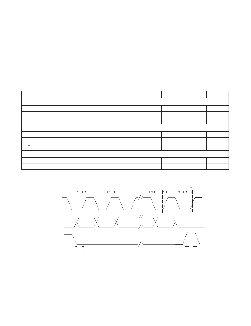
Serial programming bus
The serial input is a 3-wire input (CLOCK, STROBE, DATA) to
program all counter divide ratios, fractional compensation DAC,
selection and enable bits. The programming data is structured into
24 bit words; each word includes 2 or 3 address bits. Figure 8
shows the timing diagram of the serial input. When the STROBE
goes active HIGH, the clock is disabled and the data in the shift
register remains unchanged. Depending on the address bits, the
data is latched into different working registers or temporary
registers. In order to fully program the synthesizer, 3 words must be
sent: C, B, and A. Table 1 shows the format and the contents of
each word. The D word is normally used for testing purposes. When
sending the B-word, data bits FC7–0 for the fractional compensation
DAC are not loaded immediately. Instead they are stored in
temporary registers. Only when the A-word is loaded, these
temporary registers are loaded together with the main divider ratio.
Serial bus timing characteristics. See Figure 8.
V
DD
= V
DDCP
=+3.0V; T
amb
= +25
°
C unless otherwise specified.
SYMBOL
PARAMETER
MIN.
TYP.
MAX.
UNIT
Serial programming clock; CLK
t
r
Input rise time
–
10
40
ns
t
f
Input fall time
–
10
40
ns
T
cy
Clock period
100
–
–
ns
Enable programming; STROBE
t
START
Delay to rising clock edge
40
–
–
ns
t
W
Minimum inactive pulse width
1/f
COMP
–
–
ns
t
SU;E
Enable set-up time to next clock edge
20
–
–
ns
Register serial input data; DATA
t
SU;DAT
Input data to clock set-up time
20
–
–
ns
t
HD;DAT
Input data to clock hold time
20
–
–
ns
Application information
SR01417
CLK
DATA
STROBE
ADDRESS
LSB
t
SU;DAT
t
HD;DAT
t
r
t
w
t
f
t
SU;E
t
START
T
cy
MSB
Figure 8.
Serial Bus Timing Diagram
相關(guān)PDF資料 |
PDF描述 |
|---|---|
| SA8027 | 2.5 GHz low voltage, low power RF fractional-N/IF integer frequency synthesizer |
| SA8027DH | 2.5 GHz low voltage, low power RF fractional-N/IF integer frequency synthesizer |
| SA8027W | 2.5 GHz low voltage, low power RF fractional-N/IF integer frequency synthesizer |
| SA8028 | 2.5 GHz sigma delta fractional-N / 760 MHz IF integer frequency synthesizers |
| SA8028W | ECONOLINE: RB & RA - Dual Output from a Single Input Rail- Power Sharing on Output- Industry Standard Pinout- 1kVDC & 2kVDC Isolation- Custom Solutions Available- UL94V-0 Package Material- Efficiency to 85% |
相關(guān)代理商/技術(shù)參數(shù) |
參數(shù)描述 |
|---|---|
| SA8027 | 制造商:PHILIPS 制造商全稱:NXP Semiconductors 功能描述:2.5 GHz low voltage, low power RF fractional-N/IF integer frequency synthesizer |
| SA8027DH | 功能描述:鎖相環(huán) - PLL DUAL FRACTIONAL N SYNTHESIZER RoHS:否 制造商:Silicon Labs 類型:PLL Clock Multiplier 電路數(shù)量:1 最大輸入頻率:710 MHz 最小輸入頻率:0.002 MHz 輸出頻率范圍:0.002 MHz to 808 MHz 電源電壓-最大:3.63 V 電源電壓-最小:1.71 V 最大工作溫度:+ 85 C 最小工作溫度:- 40 C 封裝 / 箱體:QFN-36 封裝:Tray |
| SA8027DH,512 | 功能描述:射頻無線雜項 DUAL FRACTIONAL N RoHS:否 制造商:Texas Instruments 工作頻率:112 kHz to 205 kHz 電源電壓-最大:3.6 V 電源電壓-最小:3 V 電源電流:8 mA 最大功率耗散: 工作溫度范圍:- 40 C to + 110 C 封裝 / 箱體:VQFN-48 封裝:Reel |
| SA8027DH,518 | 功能描述:鎖相環(huán) - PLL DUAL FRACTIONAL N RoHS:否 制造商:Silicon Labs 類型:PLL Clock Multiplier 電路數(shù)量:1 最大輸入頻率:710 MHz 最小輸入頻率:0.002 MHz 輸出頻率范圍:0.002 MHz to 808 MHz 電源電壓-最大:3.63 V 電源電壓-最小:1.71 V 最大工作溫度:+ 85 C 最小工作溫度:- 40 C 封裝 / 箱體:QFN-36 封裝:Tray |
| SA8027DH-T | 功能描述:鎖相環(huán) - PLL DUAL FRACTIONAL N SYNTHESIZER RoHS:否 制造商:Silicon Labs 類型:PLL Clock Multiplier 電路數(shù)量:1 最大輸入頻率:710 MHz 最小輸入頻率:0.002 MHz 輸出頻率范圍:0.002 MHz to 808 MHz 電源電壓-最大:3.63 V 電源電壓-最小:1.71 V 最大工作溫度:+ 85 C 最小工作溫度:- 40 C 封裝 / 箱體:QFN-36 封裝:Tray |
發(fā)布緊急采購,3分鐘左右您將得到回復(fù)。