- 您現(xiàn)在的位置:買賣IC網(wǎng) > PDF目錄374675 > SA571NG (ON SEMICONDUCTOR) Compandor PDF資料下載
參數(shù)資料
| 型號: | SA571NG |
| 廠商: | ON SEMICONDUCTOR |
| 元件分類: | 運動控制電子 |
| 英文描述: | Compandor |
| 中文描述: | DUAL COMPANDER, 0.02 MHz BAND WIDTH, PDIP16 |
| 封裝: | LEAD FREE, PLASTIC, DIP-16 |
| 文件頁數(shù): | 9/11頁 |
| 文件大?。?/td> | 111K |
| 代理商: | SA571NG |
SA571
http://onsemi.com
9
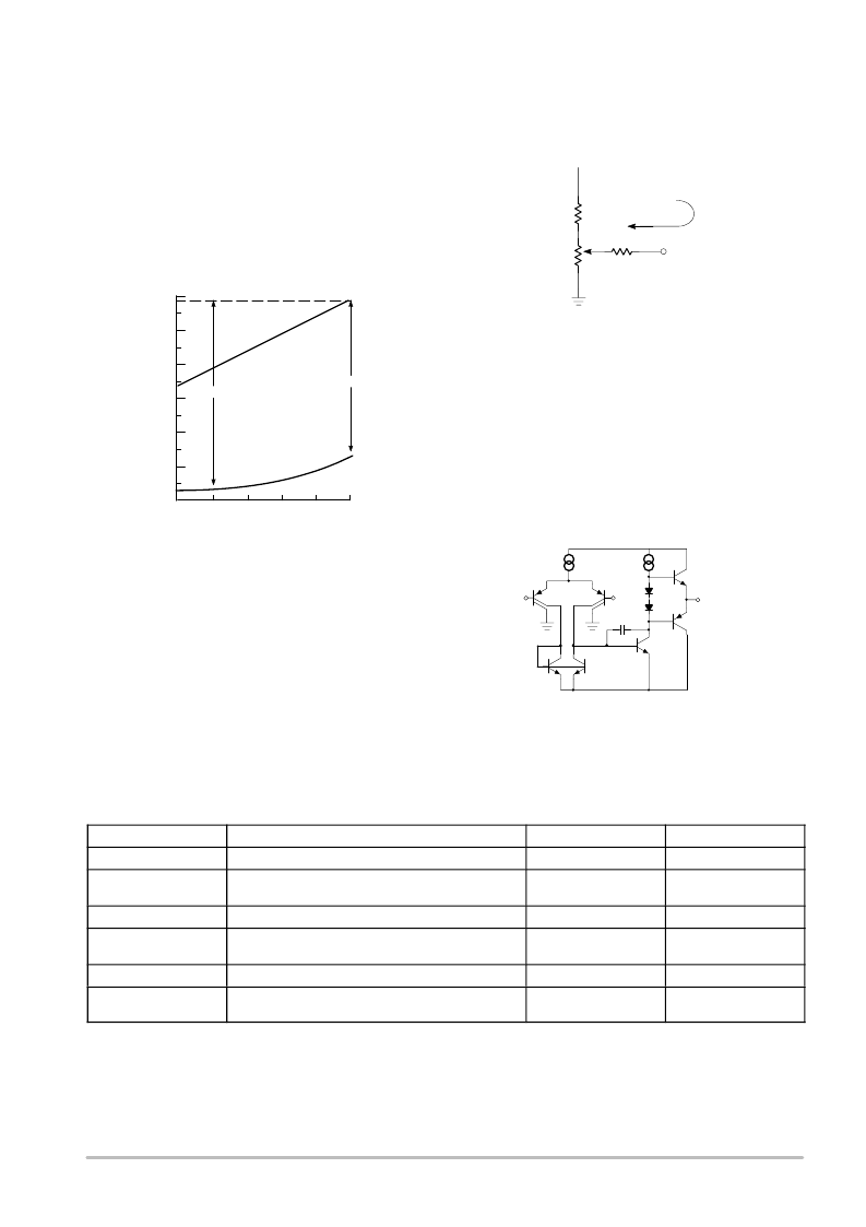
Figure 15 shows the noise performance of the G cell.
The maximum output level before clipping occurs in the
gain cell is plotted along with the output noise in a 20 kHz
bandwidth. Note that the noise drops as the gain is reduced
for the first 20 dB of gain reduction. At high gains, the signal
to noise ratio is 90 dB, and the total dynamic range from
maximum signal to minimum noise is 110 dB.
VCA GAIN (0dB)
+20
O
0
20
40
60
80
100
40
20
0
MAXIMUM
SIGNAL LEVEL
NOISE IN
20kHz BW
90dB
110dB
Figure 15. Dynamic Range
Control signal feedthrough is generated in the gain cell by
imperfect device matching and mismatches in the current
sources, I
1
and I
2
. When no input signal is present, changing
I
G
will cause a small output signal. The distortion trim is
effective in nulling out any control signal feedthrough, but
in general, the null for minimum feedthrough will be
different than the null in distortion. The control signal
feedthrough can be trimmed independently of distortion by
tying a current source to the G input pin. This effectively
trims I
1
. Figure 16 shows such a trim network.
Figure 16. Control Signal Feedthrough
RSELECT FOR
3.6V
470k
TO PIN 3 OR 14
100k
V
CC
Operation Amplifier
The main op amp shown in the chip block diagram is
equivalent to a 741 with a 1.0 MHz bandwidth. Figure 17
shows the basic circuit. Split collectors are used in the input
pair to reduce g
M
, so that a small compensation capacitor of
just 10 pF may be used. The output stage, although capable
of output currents in excess of 20 mA, is biased for a low
quiescent current to conserve power. When driving heavy
loads, this leads to a small amount of crossover distortion.
Q
1
Q
2
Q
4
Q
3
I
1
I
2
Q
6
D
1
D
2
Q
2
C
C
+IN
IN
OUT
Figure 17. Operational Amplifier
ORDERING INFORMATION
Device
Description
Temperature Range
Shipping
SA571D
16Pin Plastic Small Outline (SO16 WB) Package
40 to +85
°
C
47 Units / Rail
SA571DG
16Pin Plastic Small Outline (SO16 WB) Package
(PbFree)
40 to +85
°
C
47 Units / Rail
SA571DR2
16Pin Plastic Small Outline (SO16 WB) Package
40 to +85
°
C
1000 / Tape & Reel
SA571DR2G
16Pin Plastic Small Outline (SO16 WB) Package
(PbFree)
40 to +85
°
C
1000 / Tape & Reel
SA571N
16Pin Plastic Dual InLine Package (PDIP16)
40 to +85
°
C
25 Units / Rail
SA571NG
16Pin Plastic Dual InLine Package (PDIP16)
(PbFree)
40 to +85
°
C
25 Units / Rail
For information on tape and reel specifications, including part orientation and tape sizes, please refer to our Tape and Reel Packaging
Specifications Brochure, BRD8011/D.
相關PDF資料 |
PDF描述 |
|---|---|
| SA572DG | Programmable Analog Compandor |
| SA572DR2 | Programmable Analog Compandor |
| SA572DR2G | Programmable Analog Compandor |
| SA572DTB | Programmable Analog Compandor |
| SA572DTBG | Programmable Analog Compandor |
相關代理商/技術參數(shù) |
參數(shù)描述 |
|---|---|
| SA572 | 制造商:PHILIPS 制造商全稱:NXP Semiconductors 功能描述:Programmable analog compandor |
| SA57254-20GW | 制造商:PHILIPS 制造商全稱:NXP Semiconductors 功能描述:CMOS switching regulator (PWM controlled) |
| SA57254-25GW | 制造商:PHILIPS 制造商全稱:NXP Semiconductors 功能描述:CMOS switching regulator (PWM controlled) |
| SA57254-28GW | 制造商:PHILIPS 制造商全稱:NXP Semiconductors 功能描述:CMOS switching regulator (PWM controlled) |
| SA57254-30GW | 制造商:PHILIPS 制造商全稱:NXP Semiconductors 功能描述:CMOS switching regulator (PWM controlled) |
發(fā)布緊急采購,3分鐘左右您將得到回復。