- 您現(xiàn)在的位置:買賣IC網(wǎng) > PDF目錄374675 > SA5230 (ON SEMICONDUCTOR) Low Voltage Operational Amplifier(低壓運算放大器) PDF資料下載
參數(shù)資料
| 型號: | SA5230 |
| 廠商: | ON SEMICONDUCTOR |
| 英文描述: | Low Voltage Operational Amplifier(低壓運算放大器) |
| 中文描述: | 低電壓運算放大器(低壓運算放大器) |
| 文件頁數(shù): | 10/18頁 |
| 文件大?。?/td> | 245K |
| 代理商: | SA5230 |
NE5230, SA5230, SE5230
http://onsemi.com
10
REMOTE TRANSDUCER WITH CURRENT
TRANSMISSION
There are many ways to transmit information along two
wires, but current transmission is the most beneficial when
the sensing of remote signals is the aim. It is further
enhanced in the form of 4.0 to 20 mA information which is
used in many control
type systems. This method of
transmission provides immunity from line voltage drops,
large load resistance variations, and voltage noise pickup.
The zero reference of 4mA not only can show if there is a
break in the line when no current is flowing, but also can
power the transducer at the remote location. Usually the
transducer itself is not equipped to provide for the current
transmission. The unique features of the NE5230 can
provide high output current capability coupled with low
power consumption. It can be remotely connected to the
transducer to create a current loop with minimal external
components. The circuits for this are shown in Figures 6
and 7. Here, the part is configured as a voltage
to
current,
or transconductance amplifier. This is a novel circuit that
takes advantage of the NE5230’s large open
loop gain. In
AC applications, the load current will decrease as the
open
loop gain rolls off in magnitude. The low offset
voltage and current sinking capabilities of the NE5230 must
also be considered in this application.
The NE5230 circuit shown in Figure 6 is a pseudo
transistor configuration. The inverting input is equivalent to
the “base,” the point where V
EE
and the non
inverting input
meet is the “emitter,” and the connection after the output
diode meets the V
CC
pin is the collector. The output diode
is essential to keep the output from saturating in this
configuration. From here it can be seen that the base and
emitter form a voltage
follower and the voltage present at
R
C
must equal the input voltage present at the inverting
input. Also, the emitter and collector form a
current
follower and the current flowing through R
C
is
equivalent to the current through R
L
and the amplifier. This
sets up the current loop. Therefore, the following equation
can be formulated for the working current transmission line.
The load current is:
IL
VIN
RC
(eq. 2)
and proportional to the input voltage for a set R
C
. Also, the
current is constant no matter what load resistance is used
while within the operating bandwidth range of the op amp.
When the NE5230’s supply voltage falls past a certain point,
the current cannot remain constant. This is the “voltage
compliance” and is very good for this application because of
the near rail output voltage. The equation that determines the
voltage compliance as well as the largest possible load
resistor for the NE5230 is as follows:
[Vremote supply
RLmax
VCC min
IL
VIN max]
(eq. 3)
Where V
CC min
is the worst
case power supply voltage
(approximately 1.8 V) that will still keep the part
operational. As an example, when using a 15 V remote
power supply, a current sensing resistor of 1.0 , and an
input voltage (V
IN
) of 20 mV, the output current (I
L
) is
20 mA. Furthermore, a load resistance of zero to
approximately 650 can be inserted in the loop without any
change in current when the bias current
control pin is tied
to the negative supply pin. The voltage drop across the load
and line resistance will not affect the NE5230 because it will
operate down to 1.8 V. With a 15 V remote supply, the
voltage available at the amplifier is still enough to power it
with the maximum 20 mA output into the 650 load.
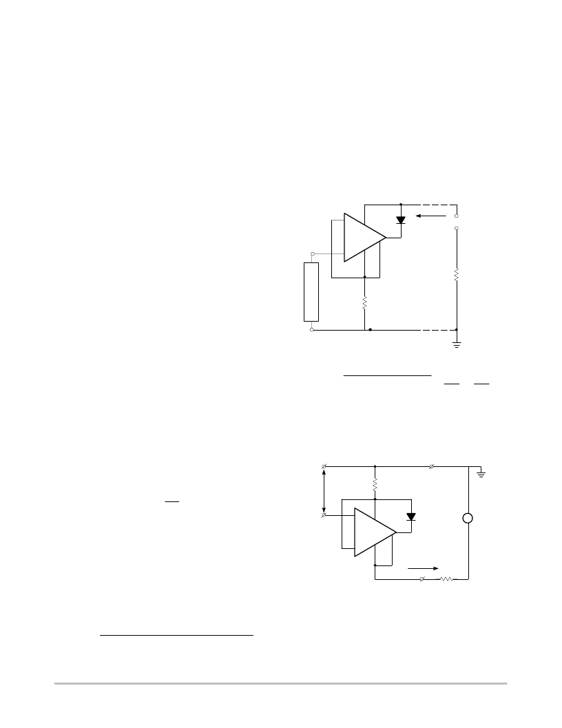
Figure 6. The NE5230 as a Remote Transducer
Transconductance Amp with 4.0
20 mA Current
Transmission Output Capability
T
R
A
N
S
D
U
C
E
R
V
REMOTE
POWER
SUPPLY
NE5230
V
CC
V
EE
V
IN
I
OUT
3
2
4
5
6
7
+
R
C
R
L
+
NOTES:
1. I
OUT
= V
IN/RC
2. R
L MAX
≈
V
REMOTE
1.8V
I
OUT
V
INMAX
For R
C
= 1.0
I
OUT
4mA
20mA
V
IN
4mV
20mV
Figure 7. The Same Type of Circuit as Figure 6, but
for Sourcing Current to the Load
V
CC
NE5230
3
2
4
5
6
7
+
V
EE
+ I
OUT
+
V
IN
R
C
R
L
V
CC
+
相關(guān)PDF資料 |
PDF描述 |
|---|---|
| SA5534A | Single Low Noise Operational Amplifier(單低噪聲運算放大器) |
| SA5534 | Single Low Noise Operational Amplifier(單低噪聲運算放大器) |
| SA56-11SRWA | 14.2mm (0.56INCH) SINGLE DIGIT NUMERIC DISPLAY |
| SA56-21EWA | 14.2mm (0.56INCH) SEVEN SEGMENT DISPLAY |
| SA56-21SRWA6 | 14.2mm (0.56INCH) SEVEN SEGMENT DISPLAY |
相關(guān)代理商/技術(shù)參數(shù) |
參數(shù)描述 |
|---|---|
| SA5230D | 功能描述:運算放大器 - 運放 1.8V Single Rail to RoHS:否 制造商:STMicroelectronics 通道數(shù)量:4 共模抑制比(最小值):63 dB 輸入補償電壓:1 mV 輸入偏流(最大值):10 pA 工作電源電壓:2.7 V to 5.5 V 安裝風(fēng)格:SMD/SMT 封裝 / 箱體:QFN-16 轉(zhuǎn)換速度:0.89 V/us 關(guān)閉:No 輸出電流:55 mA 最大工作溫度:+ 125 C 封裝:Reel |
| SA5230DG | 功能描述:運算放大器 - 運放 1.8V Single Rail to Rail Industrial Temp RoHS:否 制造商:STMicroelectronics 通道數(shù)量:4 共模抑制比(最小值):63 dB 輸入補償電壓:1 mV 輸入偏流(最大值):10 pA 工作電源電壓:2.7 V to 5.5 V 安裝風(fēng)格:SMD/SMT 封裝 / 箱體:QFN-16 轉(zhuǎn)換速度:0.89 V/us 關(guān)閉:No 輸出電流:55 mA 最大工作溫度:+ 125 C 封裝:Reel |
| SA5230DR2 | 功能描述:運算放大器 - 運放 1.8V Single Rail to RoHS:否 制造商:STMicroelectronics 通道數(shù)量:4 共模抑制比(最小值):63 dB 輸入補償電壓:1 mV 輸入偏流(最大值):10 pA 工作電源電壓:2.7 V to 5.5 V 安裝風(fēng)格:SMD/SMT 封裝 / 箱體:QFN-16 轉(zhuǎn)換速度:0.89 V/us 關(guān)閉:No 輸出電流:55 mA 最大工作溫度:+ 125 C 封裝:Reel |
| SA5230DR2G | 功能描述:運算放大器 - 運放 1.8V Single Rail to Rail Industrial Temp RoHS:否 制造商:STMicroelectronics 通道數(shù)量:4 共模抑制比(最小值):63 dB 輸入補償電壓:1 mV 輸入偏流(最大值):10 pA 工作電源電壓:2.7 V to 5.5 V 安裝風(fēng)格:SMD/SMT 封裝 / 箱體:QFN-16 轉(zhuǎn)換速度:0.89 V/us 關(guān)閉:No 輸出電流:55 mA 最大工作溫度:+ 125 C 封裝:Reel |
| SA5230FE | 制造商:PHILIPS 制造商全稱:NXP Semiconductors 功能描述:Low voltage operational amplifier |
發(fā)布緊急采購,3分鐘左右您將得到回復(fù)。