- 您現在的位置:買賣IC網 > PDF目錄372102 > SA5205AN (NXP SEMICONDUCTORS) Wide-band high-frequency amplifier PDF資料下載
參數資料
| 型號: | SA5205AN |
| 廠商: | NXP SEMICONDUCTORS |
| 元件分類: | 衰減器 |
| 英文描述: | Wide-band high-frequency amplifier |
| 中文描述: | 0 MHz - 600 MHz RF/MICROWAVE WIDE BAND LOW POWER AMPLIFIER |
| 文件頁數: | 7/14頁 |
| 文件大小: | 190K |
| 代理商: | SA5205AN |
Philips Semiconductors
Product specification
NE/SA/SE5205A
Wide-band high-frequency amplifier
1992 Feb 24
7
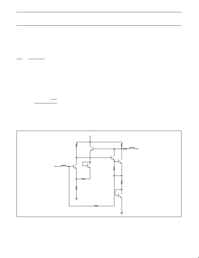
THEORY OF OPERATION
The design is based on the use of multiple feedback loops to
provide wide-band gain together with good noise figure and terminal
impedance matches. Referring to the circuit schematic in Figure 17,
the gain is set primarily by the equation:
V
OUT
V
IN
R
F1
R
E1
R
E1
(1)
which is series-shunt feedback. There is also shunt-series feedback
due to R
F2
and R
E2
which aids in producing wideband terminal
impedances without the need for low value input shunting resistors
that would degrade the noise figure. For optimum noise
performance, R
E1
and the base resistance of Q
1
are kept as low as
possible while R
F2
is maximized.
The noise figure is given by the following equation:
NF =
10 log
1
r
b
R
E1
KT
2ql
C1
R
O
dB
(2)
where I
C1
=5.5mA, R
E1
=12
, r
b
=130
, KT/q=26mV at 25
°
C and
R
0
=50 for a 50
system and 75 for a 75
system.
The DC input voltage level V
IN
can be determined by the equation:
V
IN
=V
BE1
+(I
C1
+I
C3
) R
E1
where R
E1
=12
, V
BE
=0.8V, I
C1
=5mA and I
C3
=7mA (currents rated
at V
CC
=6V).
Under the above conditions, V
IN
is approximately equal to 1V.
Level shifting is achieved by emitter-follower Q
3
and diode Q
4
which
provide shunt feedback to the emitter of Q
1
via R
F1
. The use of an
emitter-follower buffer in this feedback loop essentially eliminates
problems of shunt feedback loading on the output. The value of
R
F1
=140
is chosen to give the desired nominal gain. The DC
output voltage V
OUT
can be determined by:
V
OUT
=V
CC
-(I
C2
+I
C6
)R2,(4)
where V
CC
=6V, R
2
=225
, I
C2
=8mA and I
C6
=5mA.
From here it can be seen that the output voltage is approximately
3.1V to give relatively equal positive and negative output swings.
Diode Q
5
is included for bias purposes to allow direct coupling of
R
F2
to the base of Q
1
. The dual feedback loops stabilize the DC
operating point of the amplifier.
The output stage is a Darlington pair (Q
6
and Q
2
) which increases
the DC bias voltage on the input stage (Q
1
) to a more desirable
value, and also increases the feedback loop gain. Resistor R
0
optimizes the output VSWR (Voltage Standing Wave Ratio).
Inductors L
1
and L
2
are bondwire and lead inductances which are
roughly 3nH. These improve the high-frequency impedance
matches at input and output by partially resonating with 0.5pF of pad
and package capacitance.
V
IN
L2
3nH
Q1
Q4
RF1
140
RE1
12
RF2
200
Q5
RE2
12
R3
140
Q6
10
3nH
L2
V
OUT
R2
225
V
CC
R1
650
R0
Q3
Q2
SR00231
Figure 17. Schematic Diagram
相關PDF資料 |
PDF描述 |
|---|---|
| SA5205 | Wide-band high-frequency amplifier |
| SA5205A | Wide-band high-frequency amplifier |
| SA5209 | Wideband variable gain amplifier |
| SA5209D | Wideband variable gain amplifier |
| SA5209N | Wideband variable gain amplifier |
相關代理商/技術參數 |
參數描述 |
|---|---|
| SA5209 | 制造商:PHILIPS 制造商全稱:NXP Semiconductors 功能描述:Wideband variable gain amplifier |
| SA5209D | 制造商:PHILIPS 制造商全稱:NXP Semiconductors 功能描述:Wideband variable gain amplifier |
| SA5209D,602 | 功能描述:射頻放大器 WIDEBAND VARIABLE GAIN AMP RoHS:否 制造商:Skyworks Solutions, Inc. 類型:Low Noise Amplifier 工作頻率:2.3 GHz to 2.8 GHz P1dB:18.5 dBm 輸出截獲點:37.5 dBm 功率增益類型:32 dB 噪聲系數:0.85 dB 工作電源電壓:5 V 電源電流:125 mA 測試頻率:2.6 GHz 最大工作溫度:+ 85 C 安裝風格:SMD/SMT 封裝 / 箱體:QFN-16 封裝:Reel |
| SA5209D,623 | 功能描述:射頻放大器 WIDEBAND VARIABLE GAIN AMP RoHS:否 制造商:Skyworks Solutions, Inc. 類型:Low Noise Amplifier 工作頻率:2.3 GHz to 2.8 GHz P1dB:18.5 dBm 輸出截獲點:37.5 dBm 功率增益類型:32 dB 噪聲系數:0.85 dB 工作電源電壓:5 V 電源電流:125 mA 測試頻率:2.6 GHz 最大工作溫度:+ 85 C 安裝風格:SMD/SMT 封裝 / 箱體:QFN-16 封裝:Reel |
| SA5209N | 制造商:PHILIPS 制造商全稱:NXP Semiconductors 功能描述:Wideband variable gain amplifier |
發(fā)布緊急采購,3分鐘左右您將得到回復。